Technology · Dev
SK Hynix Opens Silicon Valley HBM Design Hub to Lock Down Next-Gen Chip Orders
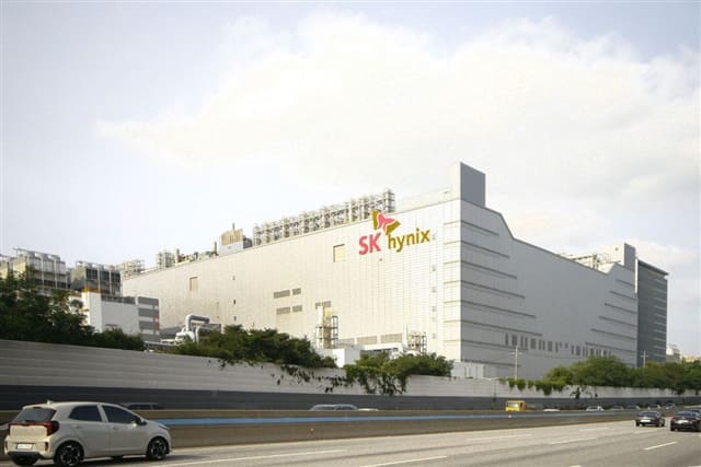
South Korean memory maker plants team near Nvidia and AMD headquarters as competition for advanced HBM4 shifts to co-design partnerships
KEY TAKEAWAYS
- ·SK Hynix is establishing a high-bandwidth memory design team in Silicon Valley to collaborate closely with major US chip customers including Nvidia and AMD.
- ·The move reflects a shift in HBM competition from manufacturing scale to co-design partnerships, as AI accelerators require tighter integration between memory and processor architectures.
- ·Winning HBM4 design-ins through early collaboration will determine memory market share for the next half-decade as suppliers race to optimize solutions for specific customer roadmaps.
A New Front in the Memory War
SK Hynix is assembling a dedicated high-bandwidth memory design team in Silicon Valley, placing engineers within reach of its largest customers. The South Korean memory giant's move signals a strategic shift in how advanced memory components are developed, as chipmakers and memory suppliers increasingly work side by side from the earliest design stages.
The new team will focus on collaborative development with major US semiconductor companies, particularly those designing AI accelerators and high-performance computing processors. By establishing a physical presence in the heart of Silicon Valley, SK Hynix aims to tighten integration cycles and reduce time-to-market for next-generation memory products.
Why Geography Matters Now
Silicon Valley hosts the headquarters and design centers of Nvidia and AMD, two of the world's most aggressive buyers of high-bandwidth memory. Nvidia's data center GPUs and AMD's Instinct accelerators both rely on HBM to feed compute cores with the massive data throughput AI workloads demand. As these processors grow more complex, memory architecture must evolve in lockstep with chip design, not as an afterthought.
Traditional development models saw memory vendors deliver standard products that chip designers then integrated. That sequential approach worked when performance requirements changed slowly. Today's AI training clusters and inference engines push bandwidth and power efficiency to new extremes every generation, making early collaboration essential. Co-design allows memory suppliers to align interface specifications, thermal profiles, and package geometries with chip roadmaps years before production.
The Co-Design Advantage
Co-design partnerships give memory makers visibility into customer roadmaps, enabling them to tailor products for specific architectures. For SK Hynix, a Silicon Valley design hub means engineers can attend weekly design reviews, iterate prototypes faster, and resolve integration issues in real time rather than through email chains spanning time zones.
This model also creates switching costs. Once a memory vendor embeds engineers inside a customer's design flow, the relationship becomes harder to displace. Competitors must offer not just better specifications on paper, but also the ability to integrate seamlessly into an existing development process.
HBM4 and the Stakes Ahead
The industry is preparing for HBM4, the next major revision of high-bandwidth memory expected to enter volume production in the coming years. HBM4 promises higher per-stack bandwidth, improved energy efficiency, and tighter integration with advanced packaging technologies. Winning design-ins for HBM4 will determine market share for the next half-decade.
SK Hynix currently holds a leading position in HBM supply, shipping large volumes to Nvidia for its H100 and H200 GPUs. Samsung and Micron are both investing heavily to close the gap, with Samsung recently announcing expanded HBM production capacity and Micron ramping its own HBM3E output. The competition is no longer only about manufacturing yield or capacity scale; it now hinges on which supplier can deliver the most optimized memory solution for each customer's architecture.
Asia's Memory Giants Go Local
SK Hynix's Silicon Valley expansion reflects a broader pattern among Asian semiconductor suppliers. Samsung operates advanced packaging and design centers in San Jose, while TSMC has built a constellation of customer support and design enablement teams across California and Texas. These investments acknowledge that proximity to customers drives better products and stickier relationships in an era when chips are too complex for arm's-length partnerships.
For SK Hynix, the move also hedges against geopolitical risk. A US-based design team can continue collaborating with American customers even if trade tensions or export controls complicate operations elsewhere. It signals commitment to the US market and aligns with Washington's push for resilient semiconductor supply chains anchored by domestic and allied partners.
What Comes Next
The establishment of SK Hynix's Silicon Valley HBM design team marks a turning point in memory competition. Success will depend less on who can build the tallest stack or the widest interface, and more on who can integrate most seamlessly into customer design flows. As AI accelerators and high-performance processors grow more specialized, memory architecture becomes inseparable from chip architecture.
Other memory vendors will face pressure to follow suit, either by opening their own design hubs near key customers or by deepening co-design partnerships through other means. The era of commodity memory is giving way to an era of bespoke memory solutions, where the closest partner often wins the order.
RELATED STORIES
Samsung Secures Pricing Leverage as 4nm Foundry Capacity Books Through 2027
Cheng Wei-Lun · 4 min
Samsung Breaks Ground on $4.3 Billion HBM Packaging Plant in South Korea
Cheng Wei-Lun · 4 min

Nvidia's Madison Huang Tours Asia Robotics Hubs in Seoul and Beijing
Cheng Wei-Lun · 3 min
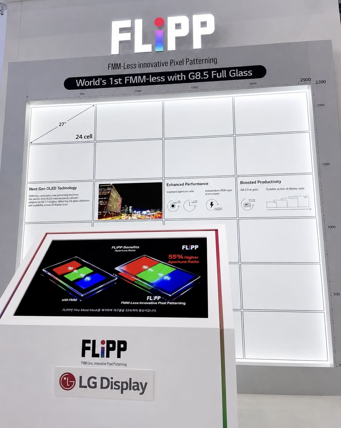
LG Display Unveils Mask-Free OLED Tech That Boosts Brightness and Lifespan
Cheng Wei-Lun · 3 min
Spot something wrong? Email editor@briefasia.com. We log every correction publicly.