Technology · Dev
Samsung Breaks Ground on $4.3 Billion HBM Packaging Plant in South Korea
The Onyang facility will combine high-bandwidth memory production with advanced packaging as the chipmaker races to catch SK hynix in the AI memory market.
KEY TAKEAWAYS
- ·Samsung Electronics will begin construction in September on a KRW6 trillion HBM production and advanced packaging facility at its Onyang campus in Asan, South Korea.
- ·The investment totals approximately $4.31 billion and aims to close the technology and market share gap with SK hynix in AI memory supply.
- ·Full volume production is targeted for 2030, positioning the plant to serve the post-2029 AI infrastructure cycle as hyperscalers deploy hundreds of thousands of accelerators.
A Bet on AI Memory Infrastructure
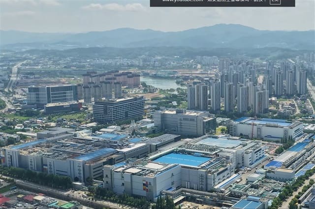
Samsung Electronics will begin construction next month on a KRW6 trillion facility dedicated to high-bandwidth memory production and advanced packaging at its Onyang campus in Asan, South Korea. The project cleared a provincial urban-planning review in August, removing the final regulatory hurdle before groundbreaking scheduled for September.
The investment, valued at approximately $4.31 billion, marks one of the largest single-site commitments Samsung has made to memory infrastructure in recent years. The Onyang site already hosts NAND flash production; the new plant will occupy adjacent land and integrate HBM fabrication with back-end packaging processes under one roof.
High-bandwidth memory has become the bottleneck component in AI accelerator systems. HBM stacks multiple DRAM dies vertically using through-silicon vias, delivering bandwidth that exceeds 1 terabyte per second in the latest generations. Nvidia, AMD, and a growing roster of AI chip designers rely on HBM to feed data-hungry training and inference workloads.
Closing the Gap with SK hynix
Samsung's move comes as the company works to close a technology and market-share gap with domestic rival SK hynix. SK hynix currently supplies the majority of HBM used in Nvidia's H100 and H200 accelerators and has secured qualification for the next-generation Blackwell platform. Samsung, by contrast, has faced delays in qualifying its fifth-generation HBM3E modules for Nvidia's systems, according to industry sources familiar with the qualification process.
The Onyang facility is designed to bring HBM production closer to packaging operations, reducing cycle time and logistics costs. Traditional memory manufacturing separates front-end wafer fabrication from back-end assembly and test, often across different sites or even countries. Co-locating these steps allows tighter process control, especially important for HBM, where thermal management and interconnect integrity are critical.
South Korea's Ministry of Trade, Industry and Energy has designated advanced packaging as a strategic priority in its semiconductor roadmap. The government plans to extend tax incentives for capital investment in packaging equipment and materials, part of a broader push to keep the country competitive against rivals in Taiwan, China, and the United States.
Regional Capacity Race
The timing of Samsung's investment reflects broader capacity additions across Asia. SK hynix is expanding HBM production at its M16 fab in Icheon and has earmarked additional cleanroom space at its Cheongju site. In Taiwan, TSMC continues to ramp advanced packaging lines for chip-on-wafer-on-substrate and other 3D integration technologies, serving both logic and memory customers.
China's CXMT and ChangXin are also investing in HBM development, though export controls on advanced packaging equipment and EDA tools have slowed progress. The U.S. Bureau of Industry and Security updated its semiconductor controls in late 2023, restricting shipments of certain hybrid-bonding and micro-bump tools to Chinese fabs.
For Samsung, the Onyang plant represents a calculated response to demand signals from hyperscale cloud operators and AI infrastructure builders. Microsoft, Amazon Web Services, Google Cloud, and Oracle have all disclosed plans to deploy hundreds of thousands of AI accelerators over the next two years. Each accelerator typically requires between 8 and 12 HBM modules, depending on configuration.
Construction Timeline and Output
Groundbreaking is set for early September, with initial cleanroom construction expected to take roughly 18 months. Equipment move-in would follow in the second half of 2028, with pilot production targeted for early 2029. Full-volume output is unlikely before 2030, meaning the facility will serve demand in the post-2029 AI infrastructure cycle rather than the current wave.
Samsung has not disclosed the plant's eventual capacity in wafer starts or module output, but industry analysts estimate the site could produce several hundred thousand HBM modules per month once fully ramped. That would represent a meaningful share of the global HBM supply base, which is currently concentrated in a handful of fabs operated by Samsung, SK hynix, and Micron.
The Asan region, where the Onyang campus is located, has emerged as a secondary semiconductor hub in South Korea, complementing the larger clusters in Pyeongtaek and Hwaseong. Local government officials have pledged infrastructure support, including expanded power substations and water treatment capacity, to accommodate the new facility's utility requirements.
Samsung's capital-expenditure cycle for memory has historically tracked DRAM and NAND pricing cycles, with investment surges following periods of tight supply and strong pricing. The current wave of spending, however, is driven less by commodity memory dynamics and more by the structural shift toward AI workloads, which demand specialized memory products with higher margins and longer qualification cycles.
The Onyang project underscores how Asia's memory producers are reconfiguring their manufacturing footprints to capture value in advanced packaging, a segment that has traditionally been dominated by outsourced assembly and test providers. By integrating packaging in-house, Samsung aims to improve yields, shorten time to market, and retain more of the margin stack in the AI memory supply chain.
RELATED STORIES
Samsung Eyes R&D Facility Conversion to Boost Foundry Output
Cheng Wei-Lun · 2 min

Samsung Fold8's Wider Aspect Ratio Pulls New Buyers into Foldable Market
Jun-ho Seo · 3 min
LG and Nvidia Push for 100,000 Hours of Humanoid Robot Training Data
Cheng Wei-Lun · 3 min
Samsung's Mobile Unit Faces 211% Memory Price Surge
Cheng Wei-Lun · 4 min
Spot something wrong? Email editor@briefasia.com. We log every correction publicly.