Technology · Dev
Samsung Eyes R&D Facility Conversion to Boost Foundry Output
The Korean chipmaker is exploring a pivot that would turn research infrastructure into production capacity amid AI-driven memory demand
KEY TAKEAWAYS
- ·Samsung is evaluating conversion of its Giheung R&D line into a foundry production facility to add advanced-node capacity.
- ·The shift reflects mounting pressure from AI memory demand and the need for faster capacity deployment than traditional fab construction allows.
- ·A final decision timeline has not been disclosed, but the move would test foundry economics and customer qualification speed.
A Rare Infrastructure Pivot
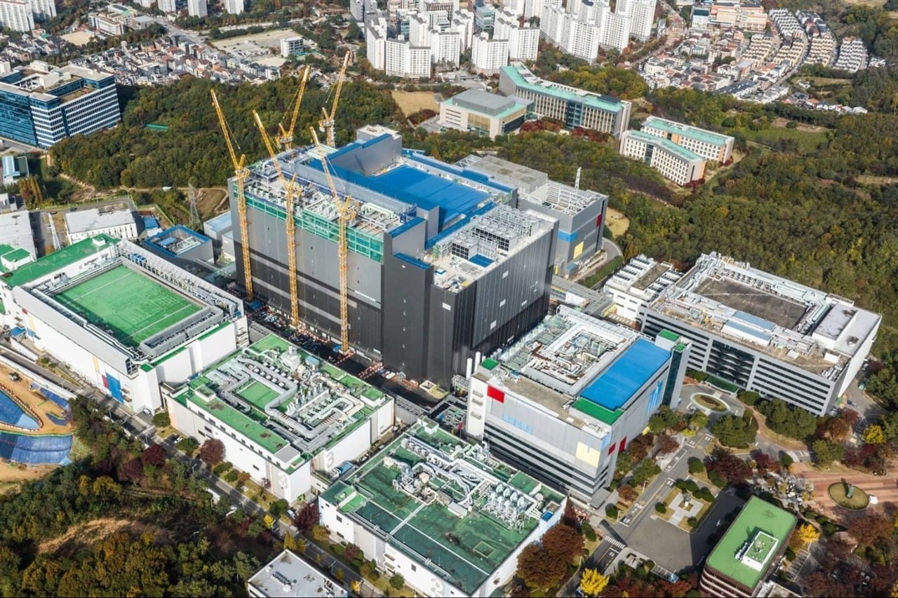
Samsung Electronics is evaluating whether to convert the second line of its next-generation semiconductor research facility in Giheung, South Korea, into a foundry production line, according to Samsung. The move would represent an unusual shift from R&D infrastructure to commercial manufacturing and signal how quickly AI memory demand is reshaping capital allocation across the industry.
The Giheung complex was designed as a testbed for advanced process development, but the company now faces competing pressures: research timelines that can absorb years of experimentation versus immediate market opportunities in 2-nanometer and below. Converting an R&D line into a so-called "send-fab" would allow Samsung to bring forward production capacity without breaking ground on entirely new facilities, a process that typically requires three to five years and tens of billions in capital expenditure.
Foundry Capacity Under Pressure
The consideration comes as Samsung and its peers navigate a structural shift in semiconductor demand. Hyperscale cloud providers and AI infrastructure builders are consuming leading-edge capacity at rates that outpace traditional product cycles. High-bandwidth memory, which pairs advanced DRAM with logic chiplets in a single package, has become a bottleneck for AI accelerator production. That bottleneck is now pulling on foundry capacity upstream.
Samsung's foundry division has lagged TSMC in winning marquee customers for the most advanced nodes, but the company has invested heavily in 3-nanometer and 2-nanometer process development. Repurposing an R&D line would let Samsung test market reception and production economics without committing to a full-scale fab expansion. It also buys time while the company finalizes yield and performance metrics that customers use to qualify vendors.
Regional Implications
The Giheung site sits at the center of South Korea's semiconductor corridor, a cluster that includes Samsung's main logic and memory fabs, as well as a dense network of equipment suppliers and materials vendors. Any capacity addition there would reinforce Korea's position in the global foundry landscape, even as the United States, Europe, and Japan roll out subsidy programs designed to pull production closer to end markets.
For Asia's chip supply chain, the move underscores a broader theme: legacy distinctions between R&D and production are blurring. Companies that once maintained strict separation between pilot lines and volume manufacturing are now treating infrastructure as fungible, reallocating cleanroom space and toolsets based on quarterly demand signals rather than multi-year roadmaps.
What Comes Next
Samsung has not disclosed a timeline for a final decision, and the company has historically run multiple scenarios in parallel before committing capital. The second line at Giheung is already equipped with some of the lithography and deposition tools needed for advanced-node production, which would lower conversion costs compared to a greenfield build. Whether the economics favor conversion will depend on how quickly Samsung can ramp yield and whether customers are willing to split orders across multiple fabs.
If Samsung proceeds, the industry will be watching two metrics closely: time to qualification and cost per wafer. Both will shape how other chipmakers think about repurposing R&D assets in an era when demand can shift faster than construction schedules allow.
RELATED STORIES
SK Keyfoundry Commits $64 Million to Expand 8-Inch Wafer Capacity
Cheng Wei-Lun · 3 min

Samsung Recruits AI Specialists to Drive Semiconductor Manufacturing Overhaul
Cheng Wei-Lun · 3 min
South Korea's Chip Design Talent Crunch Deepens as Memory Giants Chase HBM4 Engineers
Cheng Wei-Lun · 3 min
Samsung Fold8's Wider Aspect Ratio Pulls New Buyers into Foldable Market
Jun-ho Seo · 3 min
Spot something wrong? Email editor@briefasia.com. We log every correction publicly.