Technology · Dev
SK Hynix Breaks Ground on $3.9 Billion Chip Packaging Facility in Indiana
The South Korean memory chipmaker will hold its ceremony in West Lafayette on August 27, advancing its US footprint in AI-driven high-bandwidth memory production.
KEY TAKEAWAYS
- ·SK Hynix will hold a groundbreaking ceremony on August 27 for a $3.87 billion advanced packaging plant in West Lafayette, Indiana.
- ·The facility will focus on high-bandwidth memory packaging for AI accelerators, strengthening SK Hynix's position in the US supply chain.
- ·Construction timing aligns with federal CHIPS Act incentives and growing demand for HBM in data-center and AI workloads.
Construction Ceremony Set for Late August
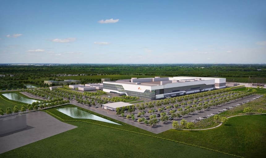
SK Hynix will officially commence construction of its advanced chip packaging facility in West Lafayette, Indiana, on August 27, according to company sources. The $3.87 billion investment marks a significant expansion of the South Korean memory manufacturer's United States operations, focused on packaging technologies for high-bandwidth memory used in artificial intelligence accelerators.
The company has begun distributing invitations to key customers and business partners for the groundbreaking event. The West Lafayette site will house both an advanced packaging facility and a research center dedicated to HBM development, positioning SK Hynix closer to major US data-center operators and AI chip designers.
Strategic Push into US AI Supply Chain
The Indiana facility represents SK Hynix's bid to secure a larger share of the rapidly growing AI chip market. High-bandwidth memory has become a critical component in training and inference workloads for large language models, with demand outstripping supply throughout 2025 and into 2026. By establishing packaging capacity on US soil, SK Hynix can reduce lead times and strengthen relationships with American hyperscalers and semiconductor designers who require tighter integration between memory and logic chips.
Advanced packaging technologies, including through-silicon vias and micro-bump interconnects, enable memory dies to be stacked vertically and bonded directly to graphics processing units or custom AI accelerators. This proximity reduces latency and increases bandwidth, both essential for the matrix operations that underpin neural network training. SK Hynix has been a leading supplier of HBM3 and HBM3E modules, competing with Samsung and Micron for contracts with firms such as NVIDIA, AMD, and emerging AI-focused fabless companies.
Timing and Regional Context
The groundbreaking ceremony arrives as the United States intensifies efforts to reshore semiconductor manufacturing and packaging. Federal incentives under the CHIPS and Science Act have catalyzed billions of dollars in announced projects across Arizona, Ohio, Texas, and now Indiana. While most attention has focused on logic fabrication, packaging remains a bottleneck in the supply chain. Memory makers have historically concentrated packaging operations in South Korea, Taiwan, and China, leaving the US with limited domestic capacity.
Indiana's selection reflects both workforce availability and proximity to Purdue University, a research institution with strengths in materials science and electrical engineering. Collaboration between industry and academia has been a recurring theme in recent semiconductor expansions, as companies seek to train the next generation of process engineers and chip designers.
Market Implications
SK Hynix's investment underscores the strategic importance of HBM in the broader memory market. While traditional DRAM and NAND products face cyclical pricing pressures, high-bandwidth memory commands premium margins due to technical complexity and tight supply. Analysts expect HBM revenue to grow at a compound annual rate exceeding 40 percent through 2028, driven by generative AI adoption across cloud computing, autonomous vehicles, and scientific research.
The West Lafayette facility will not produce memory dies themselves; those will continue to be manufactured at SK Hynix fabs in South Korea. Instead, the Indiana site will focus on the back-end assembly process, stacking dies, applying thermal interfaces, and testing finished modules before shipment to customers. This division of labor allows SK Hynix to maintain core fabrication expertise at home while addressing geopolitical and logistical concerns in the US market.
As construction begins later this month, the company will be watching how quickly it can ramp production and whether the Indiana site can meet the exacting yield requirements that HBM packaging demands. Any delays or quality issues could hand an advantage to Samsung, which is also expanding its US packaging footprint, or to Micron, which already operates memory fabs in Idaho and Virginia.
RELATED STORIES
SK Hynix Explores US Fab Sites Under Customer Pressure for Local Memory Production
Cheng Wei-Lun · 3 min

South Korea's Chip Design Talent Crunch Deepens as Memory Giants Chase HBM4 Engineers
Cheng Wei-Lun · 3 min
South Korea's Southwestern Chip Hub Set to Double in Size
Cheng Wei-Lun · 3 min
Asia's AI Chip Startups Face Manufacturing Reality Check
Priyanka V. Rao · 4 min
Spot something wrong? Email editor@briefasia.com. We log every correction publicly.