Technology · Dev
Shanghai Emerges as China's Lithography Manufacturing Center
Domestic immersion DUV systems reach mass production as equipment makers cluster in the city, accelerating Beijing's semiconductor self-sufficiency push
KEY TAKEAWAYS
- ·China has achieved mass production of domestically developed immersion DUV lithography equipment, with Shanghai emerging as the manufacturing and development hub for this technology.
- ·Shanghai Micro Electronics Equipment Group leads the effort alongside Huawei, which both uses the tools and invests in supply chains to create vertical integration.
- ·The systems target mature chip processes rather than cutting-edge nodes, reducing export control vulnerabilities while serving large automotive and industrial markets.
Manufacturing Milestone
China has achieved mass production of domestically developed immersion deep ultraviolet lithography equipment, marking a significant step in the country's effort to build indigenous semiconductor manufacturing capabilities. The systems represent the most advanced lithography tools produced within China to date, capable of patterning chips at process nodes critical for mainstream electronics.
Shanghai has emerged as the center of this activity. Multiple equipment manufacturers have concentrated operations in the municipality, creating an ecosystem that spans component suppliers, system integrators, and research institutions. The concentration mirrors patterns seen in established semiconductor equipment clusters in the Netherlands, Japan, and the United States, where proximity accelerates development cycles and knowledge transfer.
The immersion DUV technology uses water between the lens and wafer to improve resolution, enabling smaller features than dry systems. While still generations behind the extreme ultraviolet tools that produce leading-edge chips, immersion DUV remains the workhorse for memory, power semiconductors, and mature logic processes that account for the majority of global chip production by volume.
Equipment Ecosystem Takes Shape
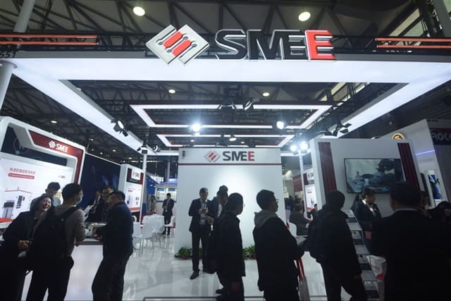
Shanghai Micro Electronics Equipment Group, known as SMEE, has been central to China's lithography ambitions since its founding in 2002. The state-backed company has steadily moved up the capability ladder, shipping its first 90-nanometer capable system in 2021 and announcing 28-nanometer targets in subsequent years. Mass production of immersion tools suggests the company has closed the reliability and throughput gaps that separate prototype systems from factory-ready equipment.
Huawei Technologies has played a dual role in this ecosystem. The telecommunications giant operates its own semiconductor design arm, HiSilicon, which became a major customer for domestic equipment after U.S. export restrictions cut access to foreign tools in 2019. Huawei has also invested in equipment supply chains, funding component makers and collaborating on tool development. This vertical integration strategy aims to create a closed loop from materials to finished chips.
Several smaller firms have entered the lithography space in recent years, targeting specific subsystems or niche applications. These companies benefit from government subsidies, access to research institutes, and a large domestic market insulated from foreign competition by both policy and geopolitics. The competitive dynamic differs sharply from global markets, where ASML dominates with over 90 percent share in advanced lithography.
Strategic Implications
Shanghai's rise as a lithography hub reflects broader patterns in China's semiconductor strategy. Rather than attempting to leapfrog directly to cutting-edge technology, authorities have prioritized building complete supply chains for mature processes. This approach reduces vulnerability to export controls while serving the large domestic market for automotive, industrial, and consumer chips that do not require leading-edge nodes.
The city offers advantages beyond manufacturing. Shanghai hosts major universities with semiconductor programs, branches of the Chinese Academy of Sciences, and a deep pool of engineering talent. Local government has provided land, tax incentives, and procurement commitments that de-risk investment. Financial markets in Shanghai have also become a key source of capital, with chip equipment firms commanding high valuations on the STAR Market.
Export restrictions imposed by the United States, Netherlands, and Japan since 2022 have accelerated localization efforts. These controls prohibit sale of advanced lithography tools to Chinese buyers, creating both urgency and political support for domestic alternatives. While the performance gap remains substantial, particularly in overlay accuracy and throughput, the existence of a domestic option changes the strategic calculus for Chinese chipmakers.
Market Realities
Mass production status indicates the equipment has passed qualification at multiple fabs, a process that typically takes 18 to 24 months and involves running thousands of wafers to verify yield and reliability. Chinese memory makers and foundries operating mature nodes are the most likely early adopters, as they face fewer alternatives and can tolerate lower throughput than cutting-edge facilities.
The systems will not displace foreign tools at fabs still able to purchase them. ASML's immersion scanners process more wafers per hour, achieve tighter tolerances, and benefit from decades of process optimization. For chipmakers balancing cost and capability, imported equipment remains the preferred choice where available.
However, the domestic tools create a floor for China's semiconductor capacity. Even if access to foreign equipment tightens further, Chinese fabs can continue expanding mature node production. This matters for applications where performance increments have slowed, such as power management, analog circuits, and legacy microcontrollers that underpin industrial and automotive systems.
Shanghai's lithography cluster is likely to deepen in the coming years. Component suppliers will co-locate to reduce logistics costs and response times. Universities will tailor programs to industry needs. Financial and legal services will specialize in semiconductor transactions. These network effects compound over time, making it harder for other cities to challenge Shanghai's position even if they offer comparable incentives.
The trajectory mirrors earlier industrial buildouts in solar panels and electric vehicle batteries, where China moved from importer to dominant producer within a decade. Lithography presents steeper technical challenges, but the combination of market scale, policy support, and export restrictions creates conditions for rapid progress within specific performance bands. Shanghai now sits at the center of that effort, translating national ambition into manufacturing reality.
RELATED STORIES
China Targets 84% Share of AR-HUD Production by 2031
Cheng Wei-Lun · 3 min

Li Auto Expands Battery Roster with CALB as Third Supplier
Siti Nuraini · 2 min
Arm Unveils Mobile Compute Platform Targeting China's AI Handset Sector
Tran Quoc Bao · 3 min
China's Battery Dominance Faces Quality Test as CALB Defect Spreads
Anand Sundaram · 3 min
Spot something wrong? Email editor@briefasia.com. We log every correction publicly.