Technology · Dev
Samsung Closes Gap on SK Hynix With Sharp HBM4 Yield Gains
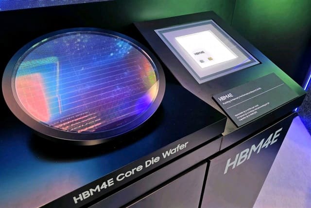
The Korean chipmaker's sixth-generation high-bandwidth memory production has reached near-80% efficiency, putting it back in the race for AI chip dominance.
KEY TAKEAWAYS
- ·Samsung Electronics has reached approximately 80% production yield for HBM4, its sixth-generation high-bandwidth memory, marking a significant improvement in manufacturing efficiency.
- ·The yield gain allows Samsung to compete more directly with SK Hynix, which has maintained a technical lead in HBM supply for AI accelerators over the past two years.
- ·High-yield HBM4 production opens the door for Samsung to secure design wins with hyperscale cloud providers and AI chip designers ahead of 2027 volume shipments.
Manufacturing Efficiency Reaches Competitive Threshold
Samsung Electronics has pushed production efficiency for its sixth-generation high-bandwidth memory to approximately 80%, a substantial jump from earlier stages of mass manufacturing. The improvement positions the company to compete more effectively on both volume output and unit economics in a market segment where SK Hynix has maintained a clear technical lead for the past two years.
High-bandwidth memory serves as the critical data pipeline for AI accelerators, feeding training and inference workloads that demand tens of terabytes per second of throughput. HBM4, the latest iteration, stacks DRAM dies vertically and connects them through thousands of through-silicon vias, a manufacturing process that is notoriously sensitive to defects. Yield rates below 70% typically make volume production uneconomical; rates above 80% signal that a manufacturer has resolved most process bottlenecks.
The Asia Memory Race Intensifies
Samsung's progress arrives at a moment when hyperscale cloud providers and AI chip designers are locking in supply agreements for 2027 delivery. Nvidia, which controls more than 80% of the data center GPU market, sources HBM from multiple vendors but has favored SK Hynix for its HBM3E products due to superior yield and thermal performance. Samsung's ability to deliver HBM4 at scale could reopen that competition.
SK Hynix began shipping HBM3E in volume in early 2025 and has maintained yields in the mid-80% range, according to industry estimates. The Icheon-based company has also secured early design wins for HBM4, which is expected to enter mass production in the second half of 2026. Samsung's yield improvements suggest it has overcome earlier challenges with die stacking alignment and thermal management, two areas where it lagged in HBM3 generations.
Cost Structure and Capacity Implications
Yield directly determines gross margin in memory manufacturing. An 80% yield means that for every 100 wafers processed, 80 meet specification and can be sold; the remaining 20 are scrapped or downgraded. At current HBM4 wafer costs estimated near $15,000 per unit, each percentage point of yield improvement translates to millions of dollars in recoverable margin across a production run.
Samsung operates DRAM fabs in Pyeongtaek and Hwaseong, with combined capacity exceeding 400,000 wafer starts per month. If the company allocates even 10% of that capacity to HBM4, it could produce several million units annually, enough to supply multiple hyperscale customers. The yield milestone suggests Samsung is ready to commit fab space at scale.
Forward Pressure on the Memory Oligopoly
The global HBM market remains tightly held by three suppliers: SK Hynix, Samsung, and Micron Technology. Micron has focused on HBM3E and has been slower to disclose HBM4 timelines. Samsung's yield recovery redistributes competitive pressure within this oligopoly, potentially constraining SK Hynix's ability to command premium pricing and forcing all three players to accelerate roadmap execution.
For customers, a second high-yield HBM4 supplier reduces concentration risk and improves negotiating leverage. For Samsung, reaching parity on yield is a necessary but not sufficient condition; it must now demonstrate reliability over sustained production runs and secure qualification from chip designers whose validation cycles can span six to nine months.
The memory industry has historically cycled between tight duopolies and brief windows of three-way competition. Samsung's HBM4 yield trajectory suggests the current window may be opening wider than many expected.
RELATED STORIES
SK Hynix Takes Top Stake in Kioxia as Toshiba Reduces Holdings
Cheng Wei-Lun · 3 min
Samsung Accelerates US Campus Recruiting to Secure Chip Talent
Cheng Wei-Lun · 3 min
Samsung Pushes Taylor Fab Qualification as 2nm Demand Reshapes US Capacity Strategy
Cheng Wei-Lun · 3 min
SK Hynix-Linked Vehicle Takes Top Stake in Kioxia as Toshiba Exits
Cheng Wei-Lun · 3 min
Spot something wrong? Email editor@briefasia.com. We log every correction publicly.