Technology · Dev
Samsung Pushes Taylor Fab Qualification as 2nm Demand Reshapes US Capacity Strategy
South Korea's chipmaker accelerates US facility certification while Seoul expands AI-focused semiconductor infrastructure to capture advanced node production
KEY TAKEAWAYS
- ·Samsung is fast-tracking qualification of its Taylor, Texas fab for 2nm production as hyperscale customers demand US-based advanced node capacity.
- ·The push reflects customer dual-sourcing strategies driven by AI workload density requirements and export control considerations.
- ·South Korea is simultaneously expanding semiconductor infrastructure with government-backed projects targeting AI accelerator production and utility capacity.
Taylor Becomes a Strategic Priority
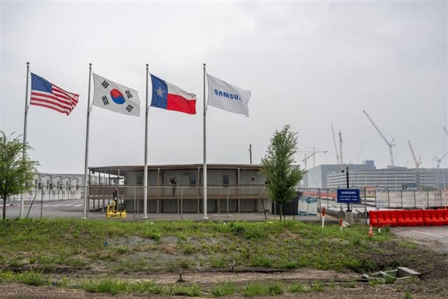
Samsung is accelerating the qualification timeline for its Taylor, Texas fabrication facility as demand for 2-nanometer process technology transforms US-based manufacturing capacity from a regional play into a strategic imperative. The South Korean semiconductor giant has intensified efforts to bring the Texas plant online for advanced node production, positioning the site to serve hyperscale cloud providers and AI chip designers seeking supply chain diversification outside Northeast Asia.
The Taylor fab, originally announced in 2021 with a projected investment exceeding $17 billion, represents Samsung's largest US manufacturing commitment. Industry observers note that the facility's certification schedule has been compressed in recent quarters, driven by customer demand for leading-edge capacity geographically separated from the company's Pyeongtaek and Hwaseong campuses in South Korea. Samsung has not disclosed a precise qualification date but has signaled readiness to ramp 2nm production in the United States by late 2026 or early 2027.
Demand Dynamics Behind the Push
The urgency reflects a broader shift in how hyperscalers and fabless chip companies evaluate supply risk. AI training and inference workloads have pushed transistor density requirements to the physical limits of current lithography, making 2nm and beyond the new battleground for performance leadership. Samsung's customers, particularly those deploying large language models and recommendation engines at scale, are pressing for capacity commitments that span multiple continents.
At the same time, export control frameworks introduced by the United States and its allies have created new friction points for cross-border chip flows. Fab capacity located within US borders offers chipmakers and their clients a measure of regulatory predictability, especially for products destined for North American data centers. Samsung's Taylor site, once viewed primarily as a hedge against geopolitical volatility, now carries commercial weight as customers formalize dual-sourcing strategies.
South Korea Expands AI Infrastructure
Parallel to the US push, South Korea has launched a series of large-scale infrastructure projects aimed at reinforcing its position as a semiconductor manufacturing hub. Government-backed initiatives are channeling capital into advanced packaging facilities, cleanroom expansions, and power infrastructure upgrades across the Gyeonggi and Chungcheong provinces. These investments are designed to support not only memory production, where South Korean firms hold dominant market share, but also logic foundry operations targeting AI accelerators and high-performance computing.
The South Korean government has committed to streamlining permitting processes for semiconductor fabs and related utilities, recognizing that speed-to-market for next-generation nodes can determine competitive outcomes. Industry groups in Seoul have called for coordinated efforts to secure supplies of ultra-pure water, industrial gases, and stable electricity, all of which are bottleneck resources for 2nm and 1.4nm production lines.
Ecosystem Reinforcement
Samsung's dual-track approach underscores a strategic shift. Rather than concentrating all advanced node capacity in a single geography, the company is building redundancy into its manufacturing footprint. The Taylor fab will serve as a western anchor, while South Korean sites retain their role as the primary R&D and high-volume manufacturing base. This distributed model allows Samsung to respond to customer preferences for supply chain resilience without sacrificing the economies of scale that come from clustering fabs near established talent pools and supplier networks.
The ecosystem play extends to equipment and materials. Suppliers of deposition tools, photoresist chemicals, and metrology systems are expanding their own US operations to support Samsung and other foundries ramping American capacity. These moves create a self-reinforcing cycle: more fabs attract more suppliers, which in turn lowers the operational friction for additional capacity investments.
What Comes Next
Samsung faces execution risk on multiple fronts. Qualifying a greenfield fab for 2nm production involves thousands of process steps, each requiring precise calibration and yield validation. Any delay in achieving target defect densities or throughput rates will ripple through customer roadmaps, potentially opening the door for competitors with more mature US footprints.
In South Korea, the challenge is sustaining momentum as infrastructure projects move from announcement to construction. Power grid upgrades and water treatment plants carry long lead times, and any shortfall in utility capacity could constrain fab ramp schedules. The government's ability to coordinate across ministries and local authorities will be tested as projects enter the execution phase.
For now, the convergence of customer demand, geopolitical considerations, and national industrial policy has aligned to make 2nm capacity a high-stakes race. Samsung's Taylor fab sits at the center of that contest, with its qualification timeline serving as a bellwether for the company's ability to compete on a global stage.
RELATED STORIES

Samsung Closes Yield Gap in Memory Race with SK Hynix
Cheng Wei-Lun · 3 min
South Korea Posts Record Early-August Export Surge on Memory Chip Demand
Cheng Wei-Lun · 3 min
Seoul Warns Against Redistributing Chip Profits as China Investment Accelerates
Jun-ho Seo · 2 min
Samsung Accelerates US Campus Recruiting to Secure Chip Talent
Cheng Wei-Lun · 3 min
Spot something wrong? Email editor@briefasia.com. We log every correction publicly.