Technology · Dev
China Moves Homegrown Immersion DUV Lithography Into Limited Production
The shift from prototype to commercial deployment marks a watershed moment in Beijing's decade-long push for semiconductor equipment self-sufficiency, though volume manufacturing remains years away.
KEY TAKEAWAYS
- ·China has transitioned domestically developed immersion DUV lithography machines from prototype to limited production, targeting nodes between 28 and 7 nanometers.
- ·Initial output will likely number single digits annually, allocated to state-backed fabs for qualification, with commercial sales not expected before 2028.
- ·The milestone arrives amid tightening export controls that bar ASML from servicing many existing DUV systems in China, accelerating the urgency of indigenous alternatives.
A Decade-Long Effort Reaches a Milestone
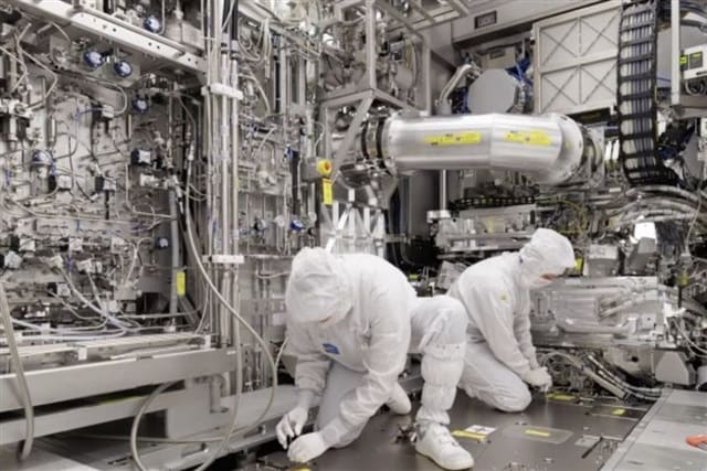
China has begun producing domestically developed immersion deep-ultraviolet lithography machines, transitioning a critical semiconductor-equipment programme from the prototype phase into limited commercial deployment. The move represents the most tangible progress yet in Beijing's efforts to build indigenous capacity in one of the most strategically sensitive corners of the chip supply chain.
Immersion DUV systems are essential for fabricating logic chips at process nodes between 28 nanometers and 7 nanometers, a range that covers a substantial share of global semiconductor output, from automotive microcontrollers to mid-tier smartphone processors. Until now, China's domestic chipmakers have depended almost entirely on equipment from ASML, the Netherlands-based monopolist in advanced lithography.
The transition to production signals that Chinese equipment makers have cleared a threshold that many Western analysts doubted they could reach before 2028. While the machines remain far from matching ASML's Twinscan NXT series in throughput or overlay precision, their existence alone reshapes the calculus for export-control policymakers in Washington, The Hague, and Tokyo.
What Limited Production Actually Means
Limited production does not imply mass deployment. Industry observers familiar with Chinese semiconductor programmes estimate that initial output will likely number in the single digits per year, with machines allocated to state-backed fabs for qualification and ramp-up testing. Full-scale commercial sales to private chipmakers are not expected before 2028, and even then, yields and reliability will need years of iteration.
The machines now entering production are believed to use a 193-nanometer argon-fluoride laser source, the same wavelength employed by ASML's DUV systems, combined with water immersion optics to boost resolution. Overlay accuracy and lens durability remain the two most challenging technical hurdles. ASML's machines achieve overlay errors below 2 nanometers; Chinese prototypes tested in 2025 were reported to fall in the 3- to 5-nanometer range, acceptable for mature nodes but insufficient for cutting-edge logic.
China's State Council identified lithography as a "chokepoint technology" in its Made in China 2025 roadmap, funneling an estimated USD 50 billion into equipment R&D through the National Integrated Circuit Industry Investment Fund. Much of that capital has flowed to Shanghai Micro Electronics Equipment, the lead developer of immersion DUV systems, which has been working on the technology since 2016.
The Geopolitical Backdrop
The production milestone arrives amid a thickening web of semiconductor export controls. In January 2026, the United States expanded its Foreign Direct Product Rule to cover immersion DUV systems with overlay precision better than 2.5 nanometers, effectively barring ASML from servicing or upgrading many of the machines already installed in China. The Dutch government has enforced parallel restrictions under its own export-licensing regime.
Those controls accelerated the urgency of China's domestic programme. Without access to ASML service contracts, Chinese fabs face a looming obsolescence problem: existing DUV tools will degrade, and replacement parts will become scarce. Indigenous alternatives, even if less capable, offer a hedge against supply cutoffs.
For Beijing, the immersion DUV programme is also a proof point for the broader substitution strategy. If China can field competitive equipment in one of the hardest categories, it strengthens the case for similar efforts in etch, deposition, and inspection tools, where the technology gap is narrower.
What Comes Next
The real test will unfold over the next 18 to 24 months. Chinese chipmakers will need to integrate the new machines into existing production lines, validate process recipes, and demonstrate that wafer yields hold up over thousands of hours of operation. Any significant defect-rate issues or downtime will force fabs to revert to imported tools, undermining the business case for domestic adoption.
Meanwhile, ASML is not standing still. The company is accelerating development of next-generation DUV systems with enhanced productivity, aiming to widen the performance gap and make Chinese alternatives less attractive even to cost-sensitive buyers. The competitive dynamic will hinge not on technical parity but on whether Chinese tools are "good enough" for the applications that matter most to domestic demand.
For the rest of Asia, the implications are mixed. Taiwan, South Korea, and Japan retain commanding leads in advanced nodes and EUV lithography, where China remains at least a decade behind. But in mature-node capacity, where much of the region's automotive and industrial chip output is concentrated, a self-sufficient China could disrupt long-standing supplier relationships and tilt regional trade flows. Policymakers in Seoul and Taipei are watching closely.
RELATED STORIES
China's Chip Makers Split Three Ways Beneath the Revenue Growth
Tran Quoc Bao · 3 min
JCET Eyes $968 Million to Scale AI Packaging Lines
Tran Quoc Bao · 3 min
Li Auto Expands Battery Roster with CALB as Third Supplier
Siti Nuraini · 2 min
BYD Sets Sights on 2 Million Overseas Sales in 2026 After Brazil, Europe Surge
Cheng Wei-Lun · 3 min
Spot something wrong? Email editor@briefasia.com. We log every correction publicly.