Technology · Dev
Chinese Chipmaker Vertilite Bets $741 Million on InP Lasers for AI Networks
Jiangsu-based optical semiconductor firm pivots from VCSELs to indium phosphide technology as AI data centers demand faster interconnects
KEY TAKEAWAYS
- ·Vertilite Semiconductor is investing CNY 5 billion in a Changzhou facility to manufacture indium phosphide laser chips for AI optical interconnects.
- ·InP lasers enable data transmission speeds beyond 800 Gbps, addressing performance requirements that silicon photonics and VCSELs struggle to meet at scale.
- ·Equipment installation begins in Q4 2026, with volume production targeted for late 2027 as Chinese firms race to reduce reliance on Japanese and US suppliers.
Strategic Shift into High-Speed Optics
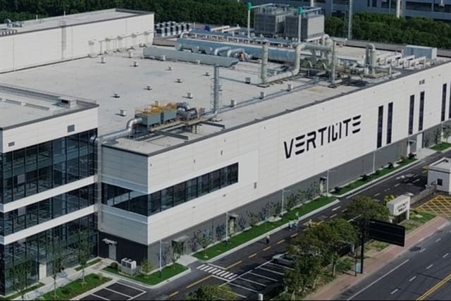
Jiangsu Vertilite Semiconductor Technology is committing CNY 5 billion (approximately $741 million) to construct a new research and manufacturing facility in Changzhou, according to the company. The investment marks a significant expansion beyond its current vertical-cavity surface-emitting laser (VCSEL) portfolio into indium phosphide laser chips designed specifically for AI optical interconnects.
The move positions the Chinese optical semiconductor manufacturer to compete in a segment where data transmission speed and power efficiency are critical. AI training clusters and hyperscale data centers increasingly rely on optical interconnects operating at 800 Gbps and beyond - speeds where traditional silicon photonics approaches face physical limitations.
Why Indium Phosphide Matters
Indium phosphide lasers offer distinct advantages over competing technologies in high-performance computing environments. The material system enables direct modulation at frequencies exceeding 50 GHz, supports wavelength-division multiplexing across wider spectral ranges, and maintains coherence over longer fiber runs - all essential characteristics for rack-to-rack and pod-to-pod communication in large AI installations.
While VCSELs have dominated short-reach datacenter links at 100 and 400 Gbps, InP-based distributed feedback lasers and electro-absorption modulated lasers are becoming the preferred solution for next-generation 1.6 Tbps and 3.2 Tbps modules. The technology also integrates more readily with coherent transmission schemes, which major cloud providers are now evaluating for intra-datacenter use.
Vertilite's timing aligns with broader industry momentum. Several Asian foundries and integrated device manufacturers have announced InP capacity expansions over the past eighteen months, driven by orders from networking equipment vendors serving hyperscalers in North America and China.
Changzhou's Growing Semiconductor Footprint
The Changzhou facility will house both R&D labs and volume production lines for communications chips and devices, according to Vertilite. Changzhou has emerged as a secondary hub for compound semiconductor manufacturing in Jiangsu province, complementing the more established clusters in Wuxi and Nanjing. Local government incentives and access to talent from nearby universities have attracted multiple optoelectronics firms to the city in recent years.
The new base represents one of the larger single private-sector commitments in China's optical communications supply chain since Beijing designated photonics as a strategic technology area in its latest five-year plan. State-backed funds and provincial investment vehicles have also channeled capital into domestic laser and photonic integrated circuit developers, aiming to reduce reliance on imports from Japan, the United States, and Europe.
Asia's Race for Optical Supremacy
China's push into InP lasers unfolds against a backdrop of intensifying regional competition. Japanese manufacturers such as Sumitomo Electric and Mitsubishi Electric have long held leading positions in high-reliability InP devices for telecom and datacenter applications. South Korean conglomerates are ramping pilot lines for co-packaged optics, while Taiwanese contract manufacturers are exploring partnerships with fabless laser design houses.
Export controls imposed by Washington on advanced semiconductor manufacturing equipment have not yet extended to compound semiconductor tools used in InP processing, leaving a window for Chinese firms to build out capacity. However, access to epitaxial reactor systems and high-resolution lithography remains a potential choke point if restrictions broaden.
For Vertilite, success will hinge on yield, reliability, and the ability to meet the stringent performance specifications that hyperscale customers demand. InP manufacturing is notoriously sensitive to defects and material uniformity, and scaling from pilot to high-volume production has proven difficult even for established players.
What Comes Next
The Changzhou project is expected to begin equipment installation in the fourth quarter of this year, with initial production targeted for late 2027. Vertilite has not disclosed customer names or volume commitments, but industry observers note that securing design wins with Chinese networking giants and domestic cloud operators will be essential to justify the scale of investment.
As AI workloads continue to grow - and with them the appetite for bandwidth - optical interconnects are shifting from a niche datacenter component to a critical enabler of compute infrastructure. Vertilite's bet on InP technology reflects a broader recognition across Asia that the next phase of digital infrastructure will be built on light, not just electrons.
RELATED STORIES
Yunnan Germanium Secures Long-Term InP Wafer Contract as AI Drives Optical Component Demand
Cheng Wei-Lun · 4 min

Wingtech Swings to Loss After Nexperia Control Fractures
Cheng Wei-Lun · 4 min
Samsung's China Revenue Surpasses US Market as Memory Demand Climbs
Cheng Wei-Lun · 3 min
Chinese Battery Makers Face Margin Pressure as Lithium Prices Drop and Tax Burden Climbs
Cheng Wei-Lun · 3 min
Spot something wrong? Email editor@briefasia.com. We log every correction publicly.