Technology · Dev
SK Hynix Sets Late-August Groundbreaking for $3.9 Billion Indiana Packaging Facility
The South Korean memory chipmaker accelerates its US manufacturing footprint with an advanced packaging plant designed to serve hyperscale customers closer to home.
KEY TAKEAWAYS
- ·SK Hynix will break ground in late August on a $3.9 billion advanced chip packaging facility in West Lafayette, Indiana, targeting volume production by late 2027.
- ·The plant will handle assembly, test, and packaging for memory products serving US hyperscalers, shortening lead times as HBM revenue is projected to exceed $30 billion in 2027.
- ·The project benefits from CHIPS Act incentives and positions Indiana as an emerging Midwest semiconductor hub alongside nearby Purdue University research infrastructure.
A Midwest Manufacturing Push
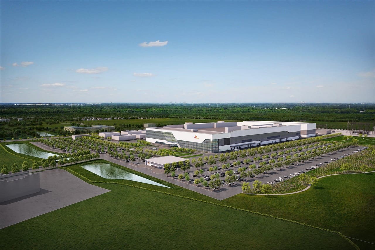
SK Hynix will hold a formal groundbreaking ceremony in late August for its $3.9 billion advanced chip packaging facility in West Lafayette, Indiana, according to the company. The project represents one of the largest foreign direct investments in the state and positions the South Korean memory giant to deliver high-bandwidth memory and other advanced products directly to US hyperscalers and cloud providers.
The West Lafayette site will focus on packaging operations rather than wafer fabrication, a strategic choice that reflects the growing complexity and value of back-end processes. Advanced packaging techniques such as through-silicon vias and hybrid bonding have become critical for stacking memory dies and connecting them to logic chips in AI accelerators. By locating packaging capacity in the United States, SK Hynix can shorten lead times and respond more quickly to design iterations from customers including Amazon Web Services, Microsoft, and Google.
Proximity to Customers and Talent
West Lafayette sits less than two hours from major data-center corridors in Illinois and Ohio, and the nearby Purdue University campus offers a steady pipeline of electrical engineering and materials science graduates. SK Hynix has already begun recruiting process engineers and equipment technicians, with plans to hire several hundred employees by the time the facility reaches volume production in late 2027.
The Indiana plant will complement SK Hynix's existing manufacturing footprint in South Korea and China, where the company produces DRAM wafers and high-bandwidth memory stacks. Packaging operations have traditionally been consolidated in Asia to benefit from supplier ecosystems and lower labor costs, but trade tensions and supply-chain resilience concerns have prompted chipmakers to diversify. Intel, TSMC, and Samsung have all announced packaging investments in the United States over the past three years, often with support from the CHIPS and Science Act.
HBM and AI Memory Demand
SK Hynix has captured the largest share of the high-bandwidth memory market, supplying HBM3 and HBM3E to Nvidia for use in H100 and H200 GPUs. Demand for these products has outstripped supply, and lead times stretched beyond six months in early 2026. The Indiana facility will not manufacture HBM dies, but it will handle final assembly, test, and packaging for a range of memory products, including modules destined for AI servers.
Industry analysts estimate that HBM revenue will exceed $30 billion in 2027, up from roughly $10 billion in 2024, driven by the rapid build-out of generative AI infrastructure. SK Hynix reported operating margins above 40 percent in its DRAM business during the first quarter of 2026, a level not seen since the previous memory super-cycle in 2018. The company has pledged to reinvest a significant portion of those profits into capacity expansion and next-generation technologies such as HBM4 and processing-in-memory architectures.
Subsidy and Incentive Framework
While SK Hynix has not disclosed the exact subsidy package tied to the Indiana project, the company is expected to receive federal grants and tax credits under the CHIPS Act, which allocated $39 billion for semiconductor manufacturing incentives. Indiana also maintains a suite of state-level programs, including property-tax abatements and workforce training grants, that have been used to attract automotive and aerospace manufacturers in recent years.
The $3.9 billion investment figure includes land acquisition, cleanroom construction, packaging equipment, and initial working capital. SK Hynix plans to complete the first phase by the end of 2027 and will evaluate a second phase depending on customer demand and the trajectory of AI chip sales. The facility is designed to be modular, allowing the company to add capacity in increments without major construction delays.
Regional Manufacturing Ecosystem
West Lafayette's emergence as a semiconductor hub reflects broader Midwest ambitions to reclaim a share of the electronics supply chain. Michigan, Ohio, and Illinois have all launched initiatives to attract chipmakers, tooling suppliers, and materials vendors. Purdue University recently opened a $100 million semiconductor research center, and several startups focused on advanced materials and metrology tools have spun out of the university's labs.
SK Hynix's Indiana plant will likely spur additional investment from packaging-materials suppliers, including substrate manufacturers and thermal-interface vendors. The company has indicated it will source some consumables locally to reduce logistics costs and improve inventory turns, a shift that could benefit regional distributors and contract manufacturers.
The late-August ceremony is expected to draw executives from SK Hynix headquarters in Seoul, Indiana's governor, and representatives from the US Department of Commerce. Construction crews have already begun site preparation, and foundation work is scheduled to start in September. If the project stays on schedule, the first packaged memory modules will leave the West Lafayette facility in the fourth quarter of 2027, marking a new chapter in the American memory industry.
RELATED STORIES
Samsung and SK Hynix Turn Down KEPCO's Multibillion-Dollar Prepayment Demand
Cheng Wei-Lun · 4 min
SK Hynix May Fast-Track Gwangju Fab Investment Alongside Yongin Expansion
Jun-ho Seo · 3 min

SK Hynix Eyes Deeper Collaboration With Japan's Chip Sector
Cheng Wei-Lun · 4 min

South Korea Records Highest September Export Start on Semiconductor Demand
Tran Quoc Bao · 3 min
Spot something wrong? Email editor@briefasia.com. We log every correction publicly.