Technology · Dev
SK Hynix Commits $38 Billion to Expand South Korean Chip Manufacturing Through 2031
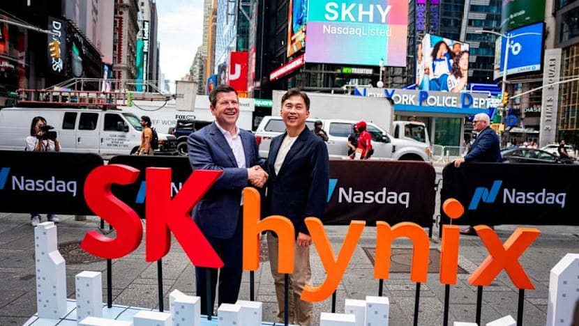
The memory chipmaker will build out production capacity in Yongin and Cheongju to meet surging AI server demand, with first cleanrooms opening from 2025
KEY TAKEAWAYS
- ·SK Hynix board approved 54.3 trillion won ($38.3 billion) in investments through 2031, split between Yongin DRAM and Cheongju NAND facilities.
- ·The Yongin Y2 fab will produce high-bandwidth memory for AI servers, with construction starting July 2025 and first cleanroom opening June 2029.
- ·SK Hynix is reviewing additional shareholder return measures, to be announced in Q3, balancing expansion with cash distributions.
Racing to Meet AI Memory Demand
SK Hynix has locked in one of the semiconductor industry's largest multi-year capital commitments, allocating 54.3 trillion won ($38.3 billion) through 2031 to expand chip production across two South Korean sites. The board approval covers 35.2 trillion won for the second fabrication plant in Yongin and 19.1 trillion won for the M17 facility in Cheongju, according to the company.
The Yongin investment centers on what SK Hynix calls the Y2 fab, the second of four planned facilities in the emerging cluster south of Seoul. That site will manufacture DRAM chips, the volatile memory that temporarily holds data for processors. DRAM has become a bottleneck in AI server builds, where models demand rapid access to vast parameter sets during inference and training runs.
Construction on Y2 is scheduled to start in July next year. The first cleanroom, the ultra-sterile space where silicon wafers are processed, is expected to open in June 2029. Production will focus on high-bandwidth memory and other advanced DRAM variants tailored for data-center accelerators.
The first Yongin fab, meanwhile, remains on schedule. SK Hynix said its initial cleanroom will open in February next year, bringing the cluster's first production capacity online ahead of the second phase.
Balancing DRAM and NAND
The Cheongju allocation targets a different segment. The M17 fab will produce NAND flash memory, the non-volatile storage used in solid-state drives for personal computers, smartphones, and increasingly AI servers that require fast local storage for model checkpoints and datasets.
Construction in Cheongju is set to begin in February next year, with the first cleanroom scheduled for December 2028. The timeline suggests SK Hynix is staging its capacity additions to match anticipated demand curves across both memory types.
The Cheongju expansion builds on an existing production base. In June, SK Hynix outlined plans to invest 100 trillion won in the city over time, alongside a much larger 600 trillion won commitment to the Yongin semiconductor cluster. The board approvals announced this week represent the first tranche of those long-term pledges, with detailed schedules and investment phases now formalized.
Capital Discipline and Shareholder Returns
SK Hynix filed a separate regulatory notice indicating it is reviewing additional shareholder return measures to enhance value. The company expects to finalize and announce details in the third quarter. The timing aligns with a broader industry pattern: chipmakers posting record margins from AI-related sales are under pressure to balance aggressive capital expenditure with cash distributions.
Memory chip prices have climbed over the past year as hyperscalers compete for HBM supply. That pricing power has improved cash flow, giving SK Hynix room to fund both multi-decade fab projects and near-term returns. The company has not disclosed what form the shareholder measures might take, whether buybacks, special dividends, or adjustments to regular payout ratios.
South Korea's Semiconductor Cluster Strategy
The Yongin and Cheongju investments fit within South Korea's national semiconductor strategy, which aims to concentrate advanced chipmaking in regional hubs supported by tax incentives and infrastructure spending. Yongin, in particular, is envisioned as a mega-cluster housing multiple fabs, research facilities, and supplier operations within commuting distance of Seoul.
SK Hynix's staggered construction schedule spreads capital outlays and labor demand across several years, reducing bottlenecks in cleanroom construction and equipment procurement. The phased approach also allows the company to adjust specifications for later fabs as memory architectures evolve and customer requirements shift.
The Cheongju site, already home to existing NAND lines, benefits from established utility connections and workforce infrastructure. Expanding there rather than opening a greenfield location accelerates time to production and lowers per-wafer costs by leveraging shared services.
With first production from the initial Yongin fab due in early 2025 and subsequent facilities coming online through 2029, SK Hynix is positioning itself to capture a larger share of the AI memory market just as the current wave of data-center buildouts matures and a second wave, driven by edge AI and on-device models, begins to take shape.
RELATED STORIES
Seoul Rejects Profit-Sharing Pressure on Samsung and SK Hynix
Cheng Wei-Lun · 3 min
SK Hynix Eyes Stake Sale in $3 Billion China Packaging Facility
Cheng Wei-Lun · 2 min
LG Uplus Hits Record Quarterly Profit as AI Data Centers Offset Revenue Dip
Cheng Wei-Lun · 3 min
South Korea Mobilizes Conglomerates for Humanoid Robot Push
Cheng Wei-Lun · 3 min
Spot something wrong? Email editor@briefasia.com. We log every correction publicly.