Technology · Dev
Rapidus Projects Eight-Reticle Interposers as Chip Packaging Hits Scale Limits
Japan's semiconductor venture sees advanced packaging pushing beyond conventional wafer economics as chiplet architectures and memory bandwidth demands grow
KEY TAKEAWAYS
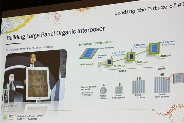
- ·Rapidus projects interposers for high-performance chips will reach eight-reticle scale by around 2030, driven by larger chiplet designs and high-bandwidth memory integration.
- ·Eight-reticle packages strain conventional 300mm wafer economics, reducing usable units per wafer and increasing per-unit costs as package footprints expand.
- ·The timeline aligns with Rapidus's 2nm logic ramp and Japan's broader strategy to re-enter cutting-edge semiconductor manufacturing through vertical integration of logic and packaging.
Manufacturing Economics Under Pressure
Rapidus anticipates that interposers for high-performance computing chips will expand to eight-reticle configurations by approximately 2030, according to the company. The projection reflects a structural shift in advanced packaging as chiplet designs and high-bandwidth memory integration drive substrate dimensions toward limits that strain conventional 300mm wafer production economics.
An eight-reticle interposer represents a significant escalation in scale. Each reticle field on a photolithography stepper covers a fixed area; an eight-reticle design implies a package footprint that spans eight times that base unit. At that scale, the number of usable interposers per wafer drops sharply, raising per-unit costs and complicating yield management. For context, current leading-edge packages typically employ two to four reticles. Moving to eight signals that designers are prioritizing performance bandwidth over manufacturing efficiency.
Chiplet Architectures Drive Substrate Expansion
The forecast from Rapidus ties directly to the trajectory of chiplet-based system architectures. Chiplets allow designers to combine multiple silicon dies, often built on different process nodes, into a single package. This approach sidesteps the yield penalties and cost walls of monolithic designs at advanced nodes. However, it demands larger interposers to accommodate more dies, wider interconnect fabrics, and additional stacks of high-bandwidth memory.
High-bandwidth memory in particular consumes substantial real estate. Each HBM stack measures several square millimeters, and leading-edge AI accelerators and data center processors now integrate multiple stacks to feed compute units with terabytes per second of bandwidth. As HBM generations advance and stack counts rise, the interposer must grow proportionally to maintain signal integrity and thermal performance.
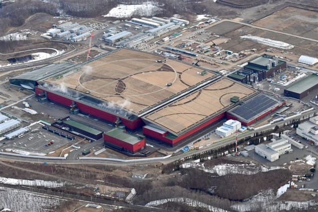
Rapidus, the Japanese semiconductor manufacturing venture backed by the government and a consortium including Toyota, Sony, and NTT, has positioned itself at the intersection of advanced logic and packaging. The company is building a fabrication facility in Hokkaido targeting sub-2nm process technology and aims to integrate leading-edge packaging capabilities within the same ecosystem. Its interposer roadmap reflects both technical ambition and a recognition that Asia's semiconductor supply chain must address packaging bottlenecks to capture value in AI and hyperscale computing markets.
Wafer Economics and the 300mm Ceiling
Standard semiconductor fabs operate on 300mm wafers, a format that has anchored manufacturing economics for two decades. Larger packages reduce the number of dies or interposers that fit on each wafer, eroding economies of scale. An eight-reticle interposer would occupy a substantial fraction of a 300mm wafer, leaving limited room for multiple units and increasing sensitivity to defects.
This dynamic is already visible in the packaging roadmaps of Taiwan and South Korea. TSMC has developed fan-out and CoWoS packaging platforms that push reticle counts upward, while Samsung has invested in interposer and panel-level packaging to address similar constraints. Panel-level packaging, which uses larger glass or organic substrates instead of silicon wafers, offers one potential path to better economics at extreme scales. Whether Rapidus will pursue panel formats or optimize within the 300mm envelope remains an open question.
Strategic Implications for Japan's Semiconductor Revival
The eight-reticle target underscores Rapidus's strategy to compete not on legacy nodes but on the cutting edge of integration. Japan's semiconductor industry ceded leadership in logic manufacturing over the past two decades, but the government's Rapidus initiative represents a deliberate attempt to re-enter at the technology frontier. Packaging represents a more accessible entry point than leading-edge logic, given lower capital intensity and shorter development cycles.
Rapidus's interposer timeline also aligns with broader regional competition. China has accelerated investment in advanced packaging as export controls limit access to cutting-edge lithography tools. South Korea and Taiwan continue to expand CoWoS, HBM integration, and hybrid bonding capabilities. Japan's bet is that vertical integration of logic, packaging, and memory within a single domestic ecosystem can create differentiation for customers seeking supply chain resilience and co-design flexibility.
What to Watch Through 2030
The path to eight-reticle interposers will test both technical feasibility and market demand. Chiplet standards, including UCIe and CXL, must mature to enable heterogeneous integration at scale. HBM supply, currently concentrated in South Korea, will need to expand to support volume production. And customers must demonstrate willingness to absorb the cost premium that comes with larger, more complex packages.
Rapidus's timeline places the eight-reticle milestone in the same window as the company's planned ramp of 2nm logic production. If both efforts converge successfully, Japan will have re-established a position in the most capital-intensive and technically demanding segment of the semiconductor value chain. If not, the interposer forecast may serve as a reminder that ambition in semiconductor manufacturing requires not only technology but also sustained capital, talent, and customer commitment.
RELATED STORIES
Rapidus Builds Packaging and Analysis Facilities at Hokkaido Semiconductor Hub
Cheng Wei-Lun · 3 min
TSMC and Sony Launch $4.69 Billion Sensor Joint Venture in Japan
Cheng Wei-Lun · 3 min
Kioxia Readies PCIe Gen6 Optical SSD for Customer Testing
Cheng Wei-Lun · 2 min

Formosa Plastics and Daicel Launch Chip Materials Joint Venture in Taiwan
Cheng Wei-Lun · 3 min
Spot something wrong? Email editor@briefasia.com. We log every correction publicly.