Technology · Dev
Rapidus Builds Packaging and Analysis Facilities at Hokkaido Semiconductor Hub
Japan's state-backed chipmaker expands its northern fab complex with advanced packaging and testing infrastructure to support domestic semiconductor ambitions
KEY TAKEAWAYS
- ·Rapidus is constructing packaging and analytical facilities at its Hokkaido semiconductor complex to create an integrated production hub beyond wafer fabrication.
- ·The expansion supports Japan's strategy to rebuild advanced chip capacity, with the government committing over 920 billion yen in subsidies to Rapidus since 2022.
- ·Adding in-house packaging reduces reliance on third-party providers in Taiwan and Southeast Asia while enabling tighter integration for multi-die chip architectures.
Expanding the Northern Complex
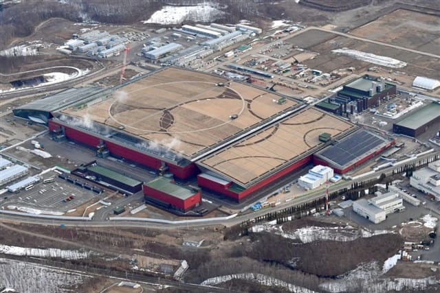
Rapidus has begun construction on additional facilities at its Hokkaido semiconductor site, extending the complex beyond wafer fabrication to include advanced packaging and analysis infrastructure. The Tokyo-headquartered chipmaker, backed by Japanese government funds and eight domestic corporations including Toyota and Sony, is positioning the northern island campus as an integrated production hub capable of handling chips from fabrication through final assembly.
The new buildings will house equipment for advanced packaging processes, which stack or connect multiple chips into single modules, alongside analytical laboratories for quality control and process development. Packaging has emerged as a critical bottleneck in semiconductor supply chains, particularly for high-performance computing and AI accelerators where chiplet architectures require precise interconnection at micrometer scales.
Hokkaido's cold climate and stable geology have made it an attractive location for precision manufacturing. The site benefits from lower ambient temperatures that reduce cooling costs for fabs, which can consume megawatts of power maintaining cleanroom environments below 20 degrees Celsius. Seismic stability relative to Japan's Pacific coast also lowers risk for the vibration-sensitive lithography tools that pattern nanometer-scale transistor features.
Japan's Semiconductor Rebuild
Rapidus was established in 2022 with the explicit mandate to restore Japan's position in leading-edge logic chips, a segment where the country lost ground over three decades as TSMC and Samsung advanced to sub-3nm nodes. The company aims to manufacture 2nm chips by 2027, leveraging technology partnerships with IBM and Imec, the Belgium-based research consortium.
The Japanese government has committed more than 920 billion yen in subsidies to Rapidus through multiple funding rounds, viewing domestic semiconductor capacity as essential to economic security. Tokyo's strategy also includes attracting foreign fabs: TSMC is building a facility in Kumamoto with Sony and Denso, while Texas Instruments has announced plans for a plant in central Japan.
Adding packaging and analysis capabilities in-house allows Rapidus to reduce dependence on third-party outsourced assembly and test providers, most of which are concentrated in Taiwan, China, and Southeast Asia. Vertical integration also shortens feedback loops between fabrication and packaging teams, useful when debugging yield issues or optimizing thermal performance in multi-die packages.
Market Context and Challenges
The expansion comes as global semiconductor capital expenditure remains elevated despite cyclical downturns in consumer electronics. Hyperscalers and AI infrastructure builders continue to order advanced nodes for data center processors, sustaining demand for cutting-edge manufacturing capacity even as memory and older logic nodes face oversupply.
Rapidus faces steep competition from incumbents with decades of process refinement and established customer relationships. TSMC's Arizona fabs are ramping 4nm production, while Intel's Ohio and European projects target 2nm-class nodes in similar timeframes. Winning design wins from fabless customers will require not just matching process specifications but also demonstrating yield rates and supply reliability.
The Hokkaido site's packaging focus aligns with broader industry trends toward heterogeneous integration, where processors, memory, and specialized accelerators are combined using advanced interconnect technologies like silicon interposers or hybrid bonding. As Moore's Law scaling slows, packaging innovation has become a primary lever for performance gains, making it a strategic capability for any foundry aspiring to serve high-end customers.
Rapidus has not disclosed capital expenditure figures for the new facilities or target timelines for packaging production. The company's initial fab is scheduled to begin pilot production in late 2025, with volume manufacturing planned for 2027.
RELATED STORIES
Honda and Nissan Align on Software-Defined Vehicle Development
Cheng Wei-Lun · 2 min

Preferred Networks Eyes Public Listing to Scale AI Chip Production
Aiko Nakamura · 2 min
Kioxia Pushes Flash Memory to Replace DRAM Amid Market Squeeze
Jun-ho Seo · 3 min

Fujitsu to Exit Commodity Hardware as AI Shifts Production Strategy
Aiko Nakamura · 4 min
Spot something wrong? Email editor@briefasia.com. We log every correction publicly.