Technology · Dev
Marvell Bets Big on India With $250 Million Expansion and Workforce Surge
The chip designer is adding 240,000 square feet of R&D facilities and preparing to hire thousands more engineers as Indian teams take on full product ownership in security and networking.
KEY TAKEAWAYS
- ·Marvell Technology is investing $250 million to expand India R&D facilities and double its workforce from 2,000 to over 4,000 engineers within three years.
- ·Indian teams now hold full product ownership in data-center security, networking, and wireless rather than simply executing designs from other regions.
- ·Advanced packaging capabilities remain unavailable in India, with no local OSAT provider currently offering the 2.5D and 3D integration Marvell's AI products require.
India Becomes Product Hub, Not Just Execution Center
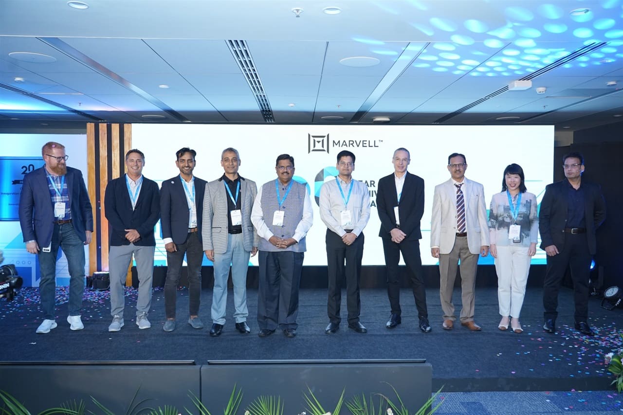
Marvell Technology has committed $250 million to expand its India operations, transforming what was once an implementation outpost into a full-fledged product development center. The semiconductor company activated 100,000 square feet of new R&D space in Bengaluru late July and is building another 265,000 square feet across its Bengaluru and Hyderabad campuses.
The three-year investment covers engineering infrastructure, product development, capital expenditure, and operational costs, according to Navin Bishnoi, Marvell's vice president and India country manager. The company intends to double its current workforce of more than 2,000 engineers, making India its second-largest R&D hub worldwide.
Marvell entered the Indian market in 2006 with a team of fewer than 50 engineers. Twenty years later, the operation spans Bengaluru, Hyderabad, and Pune, and the role has fundamentally shifted. Indian teams now hold architecture and product ownership in security, networking, wireless, and carrier infrastructure rather than simply executing designs conceived elsewhere.
Data-center security products represent one area where Indian teams drive both architecture and delivery, Bishnoi said. Foundry coordination, manufacturing, packaging, and supply-chain management remain distributed globally, but the core design work happens in India.
Custom Silicon and Hyperscaler Engagement
Hyperscalers are ordering processors tailored to specific AI workloads, and Marvell is expanding its custom-silicon business to meet that demand. Indian engineers develop subsystems that go into these chips, including memory interfaces, input-output blocks, security functions, and on-chip interconnects. These components can be configured into designs specific to individual customers.
Indian teams contribute to custom-silicon programs for hyperscalers and large enterprise clients, though no single India-based group owns an entire custom processor. Developing a full XPU can require hundreds of engineers working across IP design, electronic design automation, testing, manufacturing, and advanced packaging, making it a cross-border effort by necessity.
Marvell's Indian operations also participate in advanced process-technology projects. The company said its teams possess expertise in 2-nanometer and next-generation nodes, high-speed analog IP, subsystem development, software and firmware, and complete silicon development cycles.
AI tools are now embedded across RTL design, verification, design-for-test, physical design, firmware, and silicon validation. Verification has delivered the most significant productivity gains, followed by physical design and software development, Bishnoi said.
Packaging Remains Offshore Despite Design Growth
India's expanded role in chip design has not yet extended to local packaging and testing. Marvell is in discussions with Indian outsourced semiconductor assembly and test providers, but their current capabilities fall short of the advanced packaging required for the company's AI products.
Many Indian OSAT projects focus on mature packaging technologies. Marvell's AI chips require chiplet integration and 2.5D and 3D packaging, capabilities that no Indian OSAT currently offers or plans to deliver in the near term, Bishnoi said.
The company will continue monitoring local providers as their technology roadmaps evolve, but commercial engagement remains distant. Bishnoi expects the next phase of the India Semiconductor Mission to prioritize advanced packaging, though building the necessary ecosystem will require sustained investment and patience.
"This is a patience game," Bishnoi said, noting that developing the ecosystem would take a decade. The timeline reflects the capital intensity and technical complexity of advanced packaging, which remains concentrated in Taiwan, South Korea, and a handful of other established hubs.
Architecture Decisions Still Tied to Customer Proximity
Product-roadmap decisions generally remain close to Marvell's largest customers, many of whom are based outside India. Indian architects work directly with clients during implementation, including on custom-silicon programs, but strategic decisions are made in regions where hyperscalers and cloud providers are headquartered.
The model reflects a broader pattern in the semiconductor industry, where customer proximity continues to influence where architecture and product-planning functions sit. As Indian teams take on more product ownership, that dynamic may shift, but for now the division of labor remains tied to geography and customer relationships.
Marvell's expansion signals confidence that India can support not just cost-effective engineering talent but also the complex, multi-disciplinary work required to deliver leading-edge chips. The $250 million commitment and workforce doubling will test whether that confidence is justified.
RELATED STORIES
India's Semiconductor Push Extends to Supply Chains and Advanced Manufacturing
Priyanka V. Rao · 4 min
Indian AI Firm Commits $8 Billion to Nvidia Infrastructure Buildout
Priyanka V. Rao · 3 min
India's Semiconductor Fabs Face Critical Yield Challenge as Production Begins
Priyanka V. Rao · 4 min
Indian Chip Designer Eyes Millions in Local Wi-Fi Module Sales on CCTV Policy Push
Jun-ho Seo · 3 min
Spot something wrong? Email editor@briefasia.com. We log every correction publicly.