Technology · Dev
Kumamoto Earthquake Disrupts Japan's Semiconductor Hub With Temporary Shutdowns
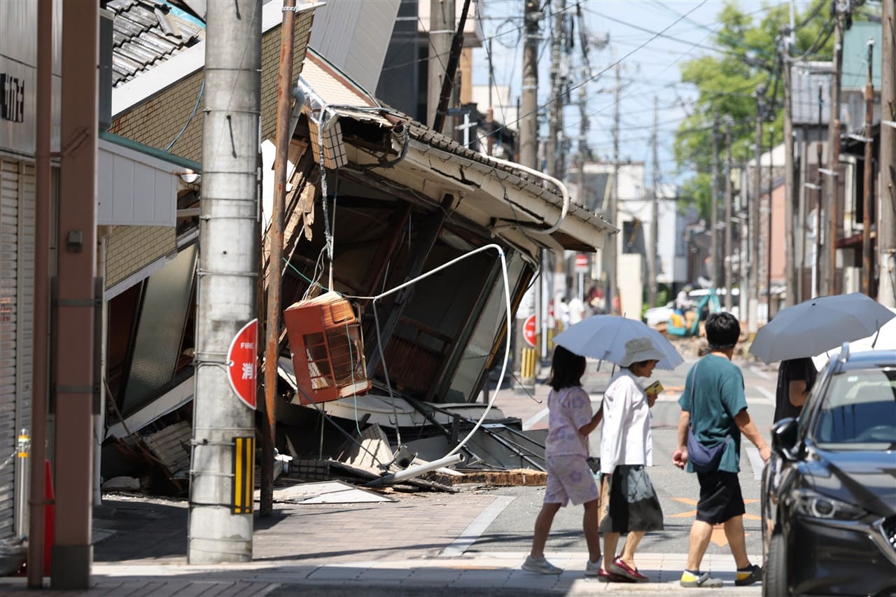
A 7.1 magnitude quake forced electronics suppliers across Kumamoto prefecture to halt operations for safety inspections, though production stoppages appear limited to precautionary measures.
KEY TAKEAWAYS
- ·A magnitude 7.1 earthquake struck Kumamoto prefecture at 4:27 p.m. on July 28, forcing electronics suppliers to evacuate staff and halt production for safety inspections.
- ·Early reports suggest most stoppages are inspection-related rather than damage-driven, typically resolving within 48 to 72 hours once facilities receive clearance.
- ·Kumamoto hosts a concentrated semiconductor cluster critical to Japan's chip ambitions, making geographic risk a key supply chain vulnerability for global electronics.
Quake Forces Cluster-Wide Safety Protocols
A magnitude 7.1 earthquake struck Japan's Kumamoto prefecture at 4:27 p.m. local time on July 28, triggering immediate production halts across the region's concentrated electronics manufacturing base. Suppliers evacuated employees and initiated facility inspections as tremors rippled through one of Asia's most critical semiconductor production zones.
The timing and location carry weight beyond the immediate disruption. Kumamoto has emerged as a focal point for Japan's semiconductor ambitions, hosting advanced fabrication facilities and a dense network of component suppliers. Any extended downtime here reverberates through global supply chains already stretched thin by capacity constraints and geopolitical fragmentation.
Inspection-Led Stoppages Dominate Early Response
Initial reports indicate that most production stoppages stem from mandatory safety inspections rather than structural damage. Electronics manufacturers across the prefecture implemented evacuation protocols and began systematic facility checks to assess equipment integrity and building safety before resuming operations.
The distinction matters for supply chain planners. Inspection-related pauses typically resolve within days once structural engineers clear facilities and equipment undergoes calibration verification. More severe scenarios involving damaged cleanrooms, misaligned lithography tools, or compromised utility infrastructure can stretch into weeks or months.
Kumamoto's semiconductor cluster includes both established Japanese manufacturers and newer entrants drawn by government incentives aimed at rebuilding domestic chip production capacity. The region's concentration of suppliers means a single seismic event can simultaneously impact multiple tiers of the electronics supply chain, from raw materials to finished components.
Regional Concentration Amplifies Risk
Japan's strategy of clustering semiconductor investment in Kumamoto creates both efficiency gains and vulnerability. Co-location reduces logistics costs and enables tighter coordination between fabs and their supplier ecosystems. But geographic concentration also means natural disasters carry outsized consequences.
The prefecture sits in a seismically active zone, with a magnitude 7.0 earthquake in 2016 causing significant damage and temporarily disrupting production at several electronics facilities. That history has pushed manufacturers to invest in seismic isolation systems and rapid inspection protocols, infrastructure now being tested again.
For multinational corporations with operations in the region, the quake underscores the challenge of balancing cost efficiency against geographic diversification. Spreading production across multiple locations increases overhead but reduces the risk that a single event paralyzes output.
Supply Chain Implications Remain Contained
The semiconductor industry's just-in-time inventory practices mean even brief production interruptions can create downstream bottlenecks. However, early indications suggest the impact remains manageable if facilities resume operations within the typical inspection window of 48 to 72 hours.
Memory and logic chip production requires ultra-clean environments and precision equipment alignment measured in nanometers. Seismic activity can disrupt both, necessitating thorough recalibration even when no visible damage occurs. This technical reality explains why semiconductor fabs often pause operations longer than other industrial facilities following earthquakes of similar magnitude.
Kumamoto's role in Japan's semiconductor ecosystem extends beyond fabrication. The prefecture hosts suppliers of specialty chemicals, precision machinery components, and testing equipment, creating a vertically integrated cluster. Disruption at any tier can cascade through the network, though the severity depends on inventory buffers and alternate sourcing options.
Asia's Seismic Manufacturing Reality
The earthquake serves as a reminder that much of Asia's electronics production sits in tectonically active regions. Taiwan, South Korea, and Japan together account for the majority of global advanced semiconductor output, and all three face regular seismic risk.
Manufacturers have responded with engineering solutions, earthquake-resistant construction, and distributed backup systems. But physics imposes limits. No amount of preparation can eliminate the need to halt operations and verify safety after a major tremor, particularly in facilities where microscopic contamination or misalignment can render entire production runs worthless.
The Kumamoto event will likely accelerate discussions around supply chain resilience and geographic diversification, themes already prominent in boardrooms and government policy circles. As semiconductor demand continues to outpace supply across multiple categories, any disruption draws scrutiny from customers dependent on steady chip flows.
For now, the focus remains on completing inspections and restarting production lines. The speed of that process will determine whether the July 28 earthquake registers as a minor hiccup or a more significant supply constraint in the quarters ahead.
RELATED STORIES

Fujitsu to Exit Commodity Hardware as AI Shifts Production Strategy
Aiko Nakamura · 4 min
Kioxia Rules Out SK Hynix Merger, Focuses on Stabilising Memory Chip Prices
Tran Quoc Bao · 3 min
Kioxia Rules Out SK Hynix Manufacturing Partnership Despite Memory Boom
Jun-ho Seo · 3 min
China Imposes Anti-Dumping Measures on Japanese Semiconductor Chemical Imports
Jun-ho Seo · 3 min
Spot something wrong? Email editor@briefasia.com. We log every correction publicly.