Technology · Products
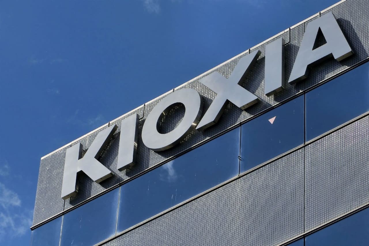
Kioxia Ships 1TB Flash Memory Samples Targeting AI-Ready Devices
Japanese memory maker delivers ninth-generation 3D flash samples as device manufacturers race to meet surging storage demands from on-device AI workloads
KEY TAKEAWAYS
- ·Kioxia has begun shipping 1TB triple-level cell memory samples built on its ninth-generation BiCS FLASH 3D architecture to device manufacturers.
- ·The new flash memory targets AI-enabled smartphones and PCs, which require higher storage capacity and faster access for on-device inference and model loading.
- ·Mass production is expected in coming quarters, aligning with flagship smartphone and premium laptop cycles planned for early 2027.
Density Push for AI Workloads
Kioxia announced it has started shipping 1TB triple-level cell memory samples to device manufacturers, built on the company's ninth-generation BiCS FLASH 3D flash architecture. The samples represent a step forward in storage capacity for consumer electronics grappling with the demands of on-device artificial intelligence, which consumes substantially more local storage than traditional applications.
The Japanese memory maker's move arrives as smartphone and PC vendors scramble to accommodate large language models, generative AI tools, and real-time inference engines that require both high-speed access and significant capacity. A 1TB module in a single package simplifies board design and frees space for other components, a priority for ultra-thin form factors.
Ninth-Generation Architecture
BiCS FLASH is Kioxia's proprietary vertical stacking approach, in which memory cells are layered upward rather than spread across a silicon wafer. Each successive generation adds more layers, increasing density without expanding the physical footprint. The ninth iteration pushes cell count higher while maintaining the triple-level cell configuration, which stores three bits per cell and strikes a balance between cost, endurance, and performance.
Triple-level cell memory sits between the faster, more expensive single-level and dual-level variants and the higher-density but slower quad-level cell designs. For AI-enabled devices that must load models quickly and write training data or cache intermediate results, triple-level cell offers a practical compromise.
Supply Chain Implications
Sampling marks the phase in which device makers test compatibility, tune controllers, and validate performance under real workloads before committing to volume orders. Kioxia's timeline suggests mass production could begin in the coming quarters, aligning with product cycles for flagship smartphones and premium laptops expected in early 2027.
The announcement also signals intensifying competition among NAND suppliers. Samsung and SK hynix have both disclosed plans for higher-layer 3D architectures, and Micron continues to refine its replacement-gate process. Kioxia's ninth-generation samples keep the company in step with rivals at a moment when memory pricing remains volatile and manufacturers seek multiple qualified sources.
Cost and Performance Outlook
Higher layer counts typically translate to lower cost per gigabyte once yields stabilize, because more capacity comes from a single wafer. That economic advantage matters for device makers targeting mid-tier and premium segments, where storage upgrades have become a key differentiation point. A 1TB option at a competitive price could accelerate the shift away from 512GB configurations, especially as operating systems and pre-installed AI features claim more base storage.
Performance gains depend not only on the memory itself but also on controller firmware and host interfaces. Kioxia has not disclosed read and write speeds for the new samples, but ninth-generation architecture is expected to deliver incremental improvements in sequential throughput and random input-output operations, both critical for AI inference and real-time data processing.
Regional Context
Asia remains the epicenter of NAND flash production, with Japan, South Korea, and Taiwan accounting for the majority of global output. Kioxia operates fabs in Yokkaichi and Kitakami, both in partnership with Western Digital, which shares the BiCS technology under a joint-development agreement. The partnership spreads capital expenditure risk and accelerates time to market, a model that has proven resilient through multiple memory cycles.
Demand from Chinese smartphone makers adds another layer of complexity. Export controls on advanced semiconductor manufacturing equipment have slowed some domestic NAND projects, leaving brands reliant on established suppliers in Japan and South Korea. Kioxia's sampling schedule positions it to capture orders from manufacturers across the region as they finalize designs for the next generation of AI-capable handsets.
What Comes Next
Device announcements in the second half of 2026 and the first quarter of 2027 will offer the clearest indication of how quickly Kioxia's ninth-generation flash reaches consumers. Flagship launches from major Android vendors and potential adoption in premium Windows laptops will test both the technical readiness of the new memory and the appetite for higher-capacity storage in markets where cloud sync has long been the default.
For now, the samples circulating among engineers represent a tangible step toward denser, faster, and more cost-effective storage, the kind of incremental advance that rarely makes headlines but quietly shapes the devices millions rely on every day.
RELATED STORIES
Kioxia Rules Out SK Hynix Merger, Focuses on Stabilising Memory Chip Prices
Tran Quoc Bao · 3 min
Kioxia Rules Out SK Hynix Manufacturing Partnership Despite Memory Boom
Jun-ho Seo · 3 min
Preferred Networks Eyes Public Listing to Scale AI Chip Production
Aiko Nakamura · 2 min
Kioxia Pushes Flash Memory to Replace DRAM Amid Market Squeeze
Jun-ho Seo · 3 min
Spot something wrong? Email editor@briefasia.com. We log every correction publicly.