Technology · Dev
India Debuts Two Silicon Photonics Tools to Bolster Local Chip Ecosystem
Indigenous platforms aim to lower barriers for researchers and industry while positioning India as an alternative node in global photonics supply chains
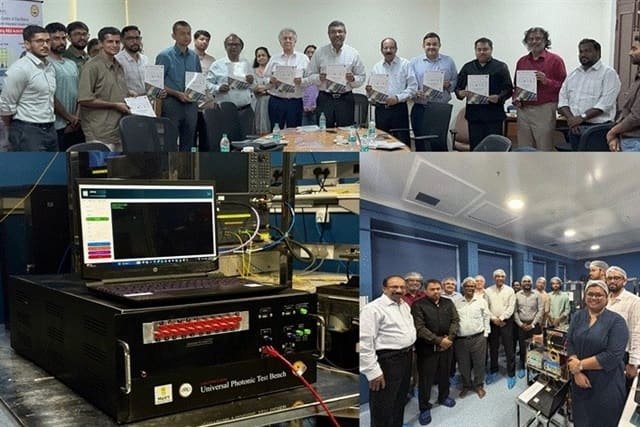
KEY TAKEAWAYS
- ·India has introduced two domestically developed silicon photonics platforms aimed at strengthening local chip design and testing capabilities for researchers and industry.
- ·The tools address access barriers in high-cost design software and characterization equipment, potentially lowering entry costs for academic labs and startups.
- ·The launch positions India as an additional node in global photonics supply chains, complementing efforts in Taiwan, South Korea, and Japan to diversify chip development hubs.
New Platforms Target Design and Testing Gaps
India has introduced two silicon photonics solutions developed domestically, marking a step toward reducing reliance on foreign chip design and testing infrastructure. The platforms are intended to support local researchers and industry players working on photonic integrated circuits, which combine optical and electronic components on a single chip.
Silicon photonics has gained traction in recent years as a technology for high-speed data transmission, sensing applications, quantum computing hardware, and advanced processing systems. By integrating light-based communication with traditional semiconductor electronics, these chips promise higher bandwidth, lower power consumption, and faster signal transmission than conventional electronic circuits alone.
The launch addresses a persistent gap in India's semiconductor ecosystem: access to specialized design tools and fabrication-testing capabilities. Until now, Indian research institutions and startups have often depended on overseas platforms or partnerships with foreign foundries to prototype and validate photonic chip designs. The new tools are designed to bring more of that workflow onshore.
Lowering the Entry Barrier
One of the key challenges in silicon photonics development is the high cost and complexity of design software and characterization equipment. Established platforms from Europe, North America, and East Asia have long dominated the market, creating barriers for researchers in emerging tech hubs who lack institutional budgets or industry partnerships.
India's homegrown solutions aim to widen access by offering domestically supported alternatives. While technical specifications and pricing details have not been disclosed, the initiative is expected to reduce dependency on imported toolchains and enable faster iteration cycles for local teams. This could prove especially valuable for academic labs and early-stage companies prototyping devices for niche applications in telecom infrastructure, medical diagnostics, and defense systems.
The move also aligns with India's broader push to build out its semiconductor manufacturing and design base. Over the past two years, New Delhi has committed billions of dollars in subsidies to attract chip fabrication plants and design centers, part of a strategy to capture a larger share of the global electronics supply chain.
Implications for Regional Supply Chains
Beyond domestic impact, India's entry into the silicon photonics tooling space could influence how global supply chains for photonic components are structured. As demand for high-performance computing, 5G and 6G networks, and quantum technologies grows, diversification of design and testing hubs has become a priority for multinational firms and governments alike.
Countries across Asia are racing to establish capabilities in advanced packaging, photonics integration, and heterogeneous chip design. Taiwan, South Korea, and Japan have already made significant investments in photonics research and production. India's new platforms add another node to the regional landscape, offering an alternative for companies seeking to de-risk supply chains or tap into lower-cost engineering talent.
The broader adoption of photonic chips hinges not only on manufacturing capacity but also on the availability of accessible design ecosystems. If India's tools prove competitive in performance and cost, they could attract international collaborators and accelerate the timeline for commercializing photonic applications in areas like lidar, optical interconnects for data centers, and biosensing.
What Comes Next
The success of these platforms will depend on adoption rates among Indian institutions and their ability to integrate with existing global workflows. Compatibility with standard fabrication processes and interoperability with international design libraries will be critical factors. Early partnerships with universities, government research labs, and private sector players will likely shape the trajectory of the initiative.
India's semiconductor ambitions face stiff competition from established players with decades of infrastructure and expertise. However, the country's large pool of electrical and photonics engineers, combined with government backing and growing private investment, provides a foundation for sustained progress. The launch of indigenous silicon photonics tools is one signal that India intends to move beyond assembly and testing into higher-value segments of the chip value chain.
For the global photonics industry, the development is a reminder that innovation hubs are proliferating beyond traditional centers. As more countries invest in specialized chip technologies, the map of where photonic devices are designed, tested, and manufactured is becoming less concentrated and more distributed.
RELATED STORIES
India's Semiconductor Push Extends to Supply Chains and Advanced Manufacturing
Priyanka V. Rao · 4 min

India's Semiconductor Fabs Face Critical Yield Challenge as Production Begins
Priyanka V. Rao · 4 min
Indian AI Firm Commits $8 Billion to Nvidia Infrastructure Buildout
Priyanka V. Rao · 3 min

Indian Chip Designer Eyes Millions in Local Wi-Fi Module Sales on CCTV Policy Push
Jun-ho Seo · 3 min
Spot something wrong? Email editor@briefasia.com. We log every correction publicly.