Technology · Dev
Hanwha Semitech Eyes FOPLP Revenue as TCB Tools Lift Q2 Earnings
South Korean equipment maker pivots to advanced packaging, with panel-level tools set to generate sales from Q3 2026 after thermocompression bonding profitability returns

KEY TAKEAWAYS
- ·Hanwha Semitech will begin booking revenue from fan-out panel-level packaging equipment in the third quarter of 2026, marking its entry into a new segment of advanced packaging tools.
- ·The South Korean equipment maker returned to profitability in the second quarter of 2026, driven by sales of thermocompression bonding tools used in high-bandwidth memory and chiplet assembly.
- ·Panel-level packaging processes promise lower per-unit costs and higher throughput than wafer-level methods, targeting OSAT customers in Taiwan, South Korea, and Southeast Asia.
Packaging Portfolio Shift
Hanwha Semitech, a South Korean semiconductor equipment supplier, is poised to book its first revenue from fan-out panel-level packaging (FOPLP) tools in the third quarter of 2026, according to the company. The milestone comes on the heels of a second-quarter swing back to profitability, powered by sales of thermocompression bonding (TCB) equipment.
The Seoul-based firm has been diversifying its product line beyond wafer-level processes, betting that advanced packaging will anchor the next phase of semiconductor miniaturization. FOPLP, which redistributes chips across large glass or organic panels before dicing, promises higher throughput and lower costs than traditional wafer-level fan-out. Hanwha's move reflects broader industry momentum: as Moore's Law economics strain, chipmakers are investing heavily in heterogeneous integration and 2.5D/3D packaging architectures.
TCB Turnaround
Thermocompression bonding, the technology that returned Hanwha to the black in Q2, is a critical enabler of high-bandwidth memory (HBM) stacks and chiplet assemblies. TCB tools use heat and pressure to form micro-bumps and hybrid bonds between dies, achieving pitch densities below 40 microns. Demand for TCB has surged alongside HBM adoption in AI accelerators; memory makers in South Korea and Taiwan have been expanding capacity to serve hyperscale data-center customers.
Hanwha's TCB sales likely benefited from this wave. The company's equipment competes with offerings from Besi and ASM Pacific Technology, both of which reported strong bonding-tool orders in the first half of 2026. Hanwha has not disclosed unit shipments or average selling prices, but industry observers note that TCB tools typically command prices in the low millions of dollars per system, with lead times stretching several quarters during peak demand.
The profitability inflection is significant for Hanwha Semitech, which had faced margin pressure through 2025 as logic-chip capital expenditure cooled. The company's parent, Hanwha Group, has been consolidating its semiconductor equipment and materials arms, aiming to build scale in a market dominated by U.S., Japanese, and Dutch incumbents.
Panel-Level Ambitions
Fan-out panel-level packaging represents a step-function leap in manufacturing efficiency. By moving from circular wafers to rectangular panels - often 510 mm × 515 mm or larger - foundries and outsourced assembly and test (OSAT) providers can process more chips per handling cycle, reducing per-unit cost. The technique is particularly attractive for applications such as radio-frequency modules, application processors for smartphones, and automotive system-on-chips, where die sizes are moderate and volume is high.
Hanwha's FOPLP equipment will likely target OSAT houses in Taiwan, South Korea, and Southeast Asia, many of which have announced pilot lines or volume ramps for panel-level processes. The company has been working with glass-substrate suppliers and mold-compound vendors to validate full process flows, a prerequisite for customer acceptance and revenue recognition.
Revenue timing is closely tied to customer qualification cycles. Equipment makers typically ship tools several quarters before recognizing revenue, as buyers run yield and reliability tests. Hanwha's Q3 2026 revenue guidance suggests that shipments occurred in late 2025 or early 2026, and that final acceptance is now imminent.
Competitive Landscape
Hanwha enters a FOPLP equipment market that remains fragmented. Incumbents include SUSS MicroTec in lithography and bonders, EV Group in panel handling, and a handful of Korean and Taiwanese toolmakers in inspection and test. No single vendor has yet established a dominant position across the full FOPLP flow, leaving room for specialists like Hanwha to carve out niches in bonding, molding, or metrology.
The company's challenge will be scaling production and service networks fast enough to meet customer roadmaps. FOPLP is still ramping; chipmakers are watching early adopters for yield data and cost validation. If panel-level processes prove out economically, equipment demand could accelerate sharply in 2027 and beyond, rewarding suppliers that have built installed bases and process knowhow.
For now, Hanwha's dual engines - TCB for high-end memory and compute, FOPLP for mid-range and mobile - offer geographic and application diversification. The company's ability to sustain profitability will hinge on execution: delivering tools on time, supporting customers through yield ramps, and investing in next-generation bonding and packaging technologies as the industry pushes toward sub-10-micron interconnects and chiplet ecosystems.
Asia's semiconductor supply chain is deepening, with equipment makers in South Korea, Taiwan, and China capturing share in segments once reserved for Japanese and American vendors. Hanwha's trajectory - from TCB recovery to FOPLP expansion - fits that pattern, underscoring the region's growing role in the capital equipment layer of the chip stack.
RELATED STORIES
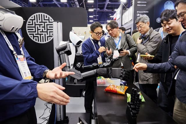
South Korea Mobilizes Conglomerates for Humanoid Robot Push
Cheng Wei-Lun · 3 min
SK Hynix Eyes Stake Sale in $3 Billion China Packaging Facility
Cheng Wei-Lun · 2 min
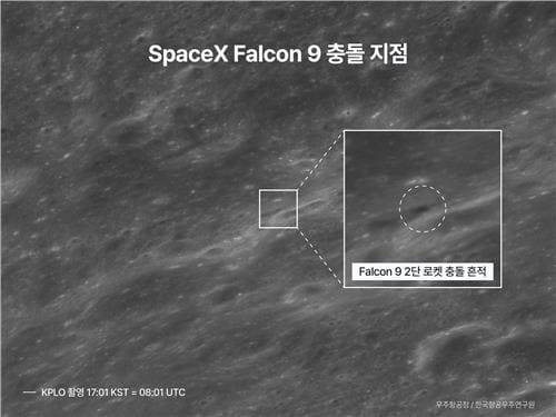
South Korea's Danuri Orbiter Photographs SpaceX Rocket Impact on Moon's Far Side
Cheng Wei-Lun · 4 min
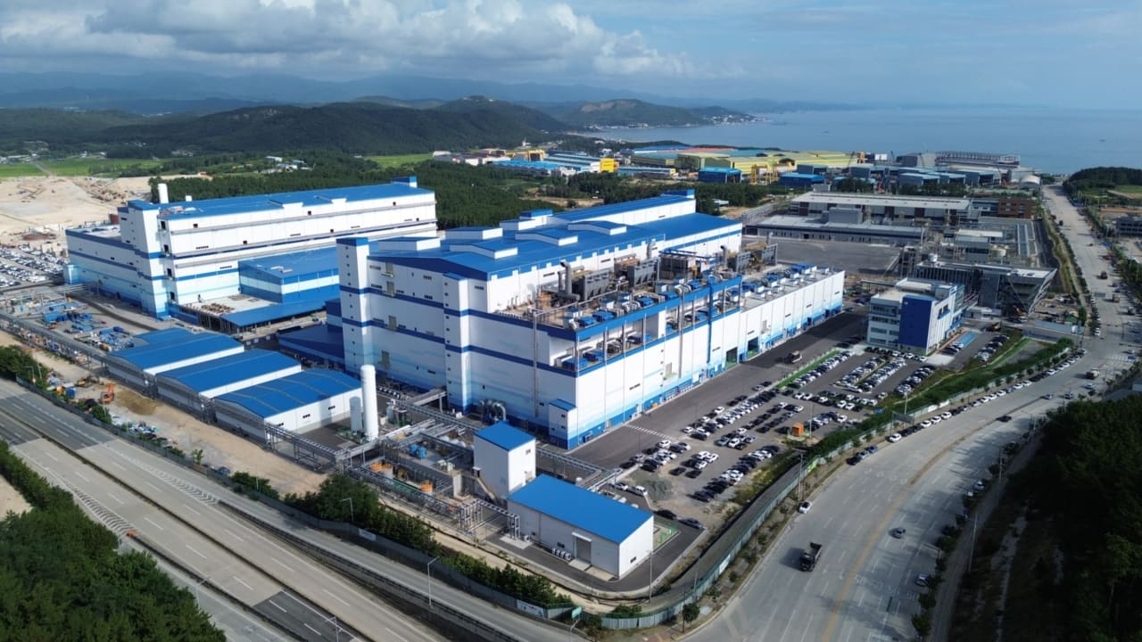
Posco Future M Lands 190,000-Ton LFP Cathode Contract in Energy Storage Push
Jun-ho Seo · 3 min
Spot something wrong? Email editor@briefasia.com. We log every correction publicly.