Technology · Dev
Korean Startup aweXome Ray Opens First Production Line for EUV Pellicle Material
Anyang-based materials company raises $5.3 million and launches commercial-scale manufacturing of carbon nanotube membranes critical to advanced chipmaking
KEY TAKEAWAYS
- ·aweXome Ray raised $5.3 million and opened a clean room production line in Anyang for carbon nanotube membranes used in EUV pellicles, moving from research to commercial manufacturing.
- ·Customer evaluations are in progress, with initial shipments expected after technical qualification, though the company did not name buyers or provide a delivery timeline.
- ·The facility addresses Korea's reliance on imported EUV pellicles and positions a local supplier within Asia's semiconductor manufacturing heartland as fabs scale sub-3nm production.
Crossing the Research Threshold
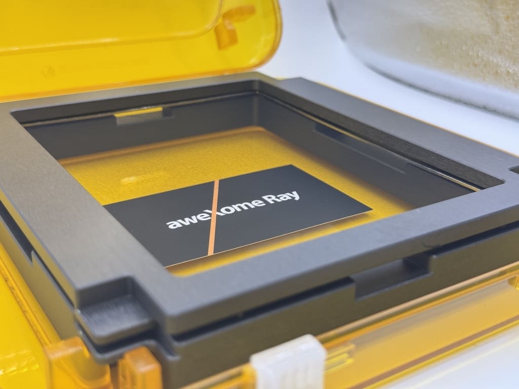
aweXome Ray announced it has completed a 7.5 billion won ($5.3 million) funding round and commissioned a clean room production line in Anyang, Gyeonggi Province, dedicated to carbon nanotube membranes for extreme ultraviolet pellicles. The facility represents the startup's transition from laboratory development to industrial-scale output, a shift that positions Korea more firmly in the specialized materials layer of semiconductor manufacturing.
Pellicles function as protective films stretched over photomasks during lithography, shielding patterns from particle contamination while allowing light to pass through. In EUV systems operating at 13.5-nanometer wavelengths, the pellicle must remain nearly transparent to minimize light loss yet mechanically robust enough to withstand the vacuum and thermal stress inside the scanner. Carbon nanotube membranes have emerged as the leading candidate material because their mesh structure combines high transmittance with tensile strength, although manufacturing them at scale with consistent quality has proved difficult.
Customer Qualification in Progress
The company said customer evaluations are currently underway, with initial shipments and revenue anticipated once those technical assessments conclude. aweXome Ray did not disclose the names of prospective buyers or provide a timeline for the start of commercial deliveries. Typical qualification cycles in semiconductor materials can span several quarters, as chipmakers and equipment vendors validate performance across dozens of parameters including transmittance uniformity, thermal expansion, and defect density.
Korea's semiconductor ecosystem has long depended on imported pellicles, primarily from suppliers in Japan and Europe. Domestic production capability addresses both supply-chain resilience and the technical coordination required when fab operators, equipment makers, and materials providers work in close geographic proximity. The Anyang line adds a local node to a supply network that has historically been concentrated outside Asia's manufacturing heartland.
EUV Lithography's Material Bottleneck
Extreme ultraviolet lithography is the enabling technology for nodes below 7 nanometers, and every leading-edge fab now relies on EUV scanners to pattern the finest features in logic and memory chips. Yet the pellicle remains one of the system's most delicate components. Early EUV production ran without pellicles because suitable materials did not exist; chipmakers accepted higher defect rates and slower throughput as the cost of pushing Moore's Law forward.
Carbon nanotube films have since matured to the point where they meet the twin requirements of transparency and durability, but the manufacturing window is narrow. The membrane must be uniform across several centimeters, free of pinholes, and stable under sustained EUV exposure. Any variation in thickness or nanotube alignment can degrade transmittance or introduce wavefront distortion, both of which erode the imaging precision that justifies EUV's capital expense.
Funding and Facility Details
The 7.5 billion won raised by aweXome Ray will support ongoing production ramp and process refinement. Clean room infrastructure for pellicle manufacturing requires stringent environmental controls, as even nanometer-scale particles can compromise membrane integrity. The Anyang facility is equipped to handle the chemical vapor deposition and transfer processes that turn carbon feedstock into free-standing nanotube films, then mount those films onto pellicle frames compatible with EUV mask pods.
Korea's materials sector has seen increased investor interest as the government prioritizes semiconductor supply-chain sovereignty. Policy initiatives including tax incentives and co-investment funds have channeled capital toward startups working on photoresists, etchants, and specialty films. aweXome Ray's funding round fits within that broader mobilization, reflecting both commercial opportunity and strategic intent.
Regional Context and Next Steps
Taiwan, Japan, and Korea together account for the majority of global advanced logic and memory capacity, yet materials supply has remained fragmented. Local production of EUV pellicles shortens the feedback loop between fab and supplier, enabling faster iteration when process changes demand material adjustments. It also reduces exposure to export restrictions and logistics delays, risks that have intensified as semiconductor technology becomes a focal point of industrial policy.
For aweXome Ray, the immediate challenge is clearing customer qualification and scaling output to meet demand from fabs running high-volume EUV production. Success will depend on yield stability, cost competitiveness, and the ability to support multiple mask formats as chipmakers diversify their lithography strategies. The company's progress will be measured not in announcements but in purchase orders, a metric that separates materials development from materials business.
RELATED STORIES
SK Hynix Reviews Future of China Packaging Facility Amid $3 Billion Valuation Talk
Cheng Wei-Lun · 2 min
Korean Builders Race to Secure Power Equipment for AI Data Centers
Jun-ho Seo · 3 min
Samsung Closes Yield Gap in Memory Race with SK Hynix
Cheng Wei-Lun · 3 min
Seoul Court Upholds Prison Term for Ex-SK Hynix Engineer in Chip Leak Case
Cheng Wei-Lun · 3 min
Spot something wrong? Email editor@briefasia.com. We log every correction publicly.