Technology · Dev
TSMC Brings 3nm Chipmaking and Advanced Packaging to Japan Expansion
The Taiwanese semiconductor giant is deepening its Kumamoto presence with cutting-edge production capabilities and sensor technology partnerships
KEY TAKEAWAYS
- ·TSMC is preparing to add 3-nanometer chip production at its Kumamoto, Japan facility, alongside advanced packaging and image sensor capabilities.
- ·The expansion positions Japan as a strategic manufacturing node for TSMC, offering customers supply redundancy outside Taiwan amid geopolitical concerns.
- ·Kumamoto will house not only cutting-edge fabrication but also packaging infrastructure, tapping into Japan's expertise in materials and precision assembly.
Taiwan Fab Giant Deepens Japan Commitment
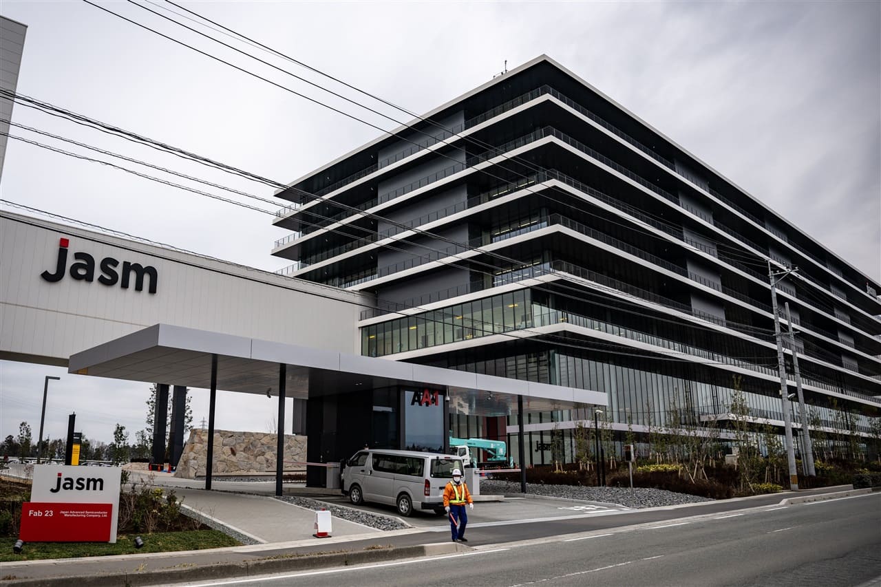
Taiwan Semiconductor Manufacturing Company is preparing to bring 3-nanometer chip production to its Kumamoto operations in Japan, according to the company. The move positions Japan as a more strategic node in TSMC's global manufacturing network, extending beyond the mature-process capacity the island nation has traditionally hosted for the foundry.
The expansion comes as TSMC continues to distribute advanced production capabilities beyond its home base in Taiwan, a shift driven by customer demand for geographic diversity and government incentives across multiple Asian markets. Japan has emerged as a beneficiary of this strategy, with Kumamoto now set to house not only 3nm fabrication but also advanced packaging infrastructure and partnerships in next-generation image sensor development.
Advanced Packaging and Design Infrastructure
Beyond the headline-grabbing 3nm fab, TSMC is establishing advanced packaging capabilities in the region, according to company announcements. Advanced packaging, which involves stacking or integrating multiple chips into a single module, has become a critical bottleneck in the semiconductor supply chain as chipmakers push the limits of traditional scaling.
The Kumamoto site will also support local chip design activities and collaboration on image sensor technology, areas where Japan retains strong domestic expertise through firms such as Sony Semiconductor Solutions. These partnerships signal TSMC's intent to embed itself more deeply into Japan's semiconductor ecosystem rather than simply operating a standalone production outpost.
Why Kumamoto Matters for TSMC's Asia Strategy
The decision to place 3nm production in Japan reflects a broader recalibration of manufacturing risk and opportunity across Asia. TSMC already operates fabs in Nanjing, China, and is building capacity in Arizona and Germany, but Japan offers a combination of political stability, technical workforce, and government co-investment that few other locations can match.
Tokyo has committed billions of dollars in subsidies to attract semiconductor manufacturing back to Japanese soil, a policy response to supply chain shocks during the pandemic and rising tensions over Taiwan. For TSMC, Kumamoto provides a hedge against geopolitical concentration while keeping production within the Asian time zone and logistics network that serves key customers including Apple, AMD, and Nvidia.
The 3nm node is currently among the most advanced in commercial production, used primarily for high-performance computing and premium smartphone processors. By replicating this capability in Japan, TSMC can offer customers a degree of supply redundancy that was previously unavailable outside Taiwan.
Local Ecosystem and Talent Pipeline
Japan's semiconductor industry, though diminished from its 1980s peak, retains pockets of deep expertise in materials, equipment, and specialized components. TSMC's expansion is designed to tap into this legacy, partnering with local suppliers and research institutions to build a vertically integrated cluster around Kumamoto.
The company has already begun hiring locally and working with Japanese universities to develop training programs tailored to advanced semiconductor manufacturing. This approach mirrors TSMC's strategy in Taiwan, where close collaboration between industry, academia, and government has sustained decades of process leadership.
Advanced packaging, in particular, benefits from proximity to design and materials expertise. Japan's strength in substrate materials and precision assembly makes it a natural location for TSMC to co-locate packaging with logic production, reducing turnaround times for customers requiring integrated solutions.
Timeline and Capacity Outlook
TSMC has not disclosed a precise timeline for when 3nm production will begin in Kumamoto, but industry observers expect the new lines to come online in phases over the next several years. The first Kumamoto fab, focused on 28nm and 22nm processes, began production in 2024 and serves automotive and industrial customers.
The addition of 3nm capacity in Japan will not replace Taiwan as TSMC's primary production base but will supplement it, particularly for customers seeking dual-sourcing options or preferring non-Taiwan exposure for strategic reasons. Packaging capabilities are expected to ramp in parallel, supporting both the local 3nm output and chips shipped from other TSMC sites.
As the semiconductor industry continues to fragment geographically, TSMC's Japan expansion underscores the foundry's willingness to invest in distributed manufacturing even as it navigates rising capital costs and uncertain demand cycles. Kumamoto's evolution from mature-node outpost to advanced-process hub reflects how quickly the strategic calculus of chipmaking has shifted across Asia.
RELATED STORIES
Asian Tech Stocks Surge as Weak US Jobs Data Dims Rate Hike Outlook
Cheng Wei-Lun · 4 min
Ajinomoto Lifts Forecast as AI Server Demand Drives Semiconductor Material Sales
Cheng Wei-Lun · 3 min
Japan Embeds Cyber Defense in Air Force Systems as AI Threats Grow
Aiko Nakamura · 4 min

Tesla Expands Japan Delivery Network to Meet Rising EV Demand
Aiko Nakamura · 3 min
Spot something wrong? Email editor@briefasia.com. We log every correction publicly.