Technology · Dev
Taiwan Emerges as Critical Hub for Co-Packaged Optics Manufacturing
Ayar Labs CEO argues the industry question has shifted from technical proof to commercial scalability, with Taiwan's packaging ecosystem positioned as the solution
KEY TAKEAWAYS
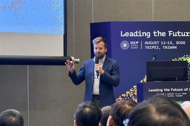
- ·Ayar Labs CEO Mark Wade stated at the 2026 OCP APAC Summit that co-packaged optics has shifted from technical validation to commercial scaling challenges.
- ·Taiwan's advanced packaging ecosystem, built around TSMC and OSAT networks, offers the process control and supply chain depth required for high-volume CPO manufacturing.
- ·Hyperscalers including Microsoft, Google, and Meta have disclosed CPO roadmaps, with the next 18 months critical for transitioning from pilot to volume production.
From Lab to Line
Co-packaged optics no longer needs to prove it works. The technology has cleared technical validation at successive industry conferences, demonstrating that integrating optical components directly with silicon can solve the bandwidth and power challenges facing hyperscale data centers. The real question now, according to Ayar Labs, is whether the industry can manufacture CPO at the volume and cost required by cloud providers and AI infrastructure operators.
Mark Wade, CEO of Ayar Labs, framed the challenge at the 2026 OCP APAC Summit. The company has moved its focus from demonstrating capability to addressing the industrial bottleneck: building a supply chain capable of producing millions of units with acceptable yields and economics.
Taiwan's Packaging Advantage
Taiwan's position in this transition stems from decades of investment in advanced packaging and heterogeneous integration. The island's semiconductor ecosystem, anchored by TSMC and a dense network of OSAT providers, has developed the process control and supply chain depth required for CPO assembly. Co-packaged optics demands tight tolerances in attaching optical dies, electrical dies, and photonic interconnects within a single package. That level of integration requires both equipment sophistication and process maturity.
Ayar Labs has identified Taiwan's packaging infrastructure as central to its commercialization strategy. The company's optical I/O chiplets, which use in-package optical links to connect processors and memory, depend on the same packaging techniques Taiwan has refined for high-bandwidth memory and chiplet architectures. The alignment tolerances for optical coupling, measured in microns, match the precision already deployed in CoWoS and similar advanced packaging platforms.
The Scaling Problem
CPO adoption hinges on cost and yield. Hyperscalers require components that can be produced at semiconductor-like volumes with failure rates low enough to justify integration at the package level. Optical components have historically been assembled by hand or in low-volume lines, a workflow incompatible with the economics of cloud infrastructure. Wade's argument is that Taiwan's packaging fabs can bring semiconductor manufacturing discipline to optics, turning a niche technology into a scalable product.
The shift matters because AI training clusters and high-performance computing systems are pushing electrical I/O to its physical limits. Copper interconnects consume increasing power as data rates rise, and signal integrity degrades over even short distances at multi-terabit speeds. CPO addresses both problems by replacing electrical links with optical ones, reducing power per bit and extending reach without retimers or signal conditioning.
Industry Momentum
Several hyperscalers have disclosed CPO roadmaps, signaling that the technology has moved from research to deployment planning. Microsoft, Google, and Meta have all participated in industry consortia developing CPO standards, and equipment vendors including Broadcom and Marvell have announced chipsets designed for co-packaged optical modules. Taiwan's role is to provide the manufacturing layer that turns those designs into products.
Ayar Labs itself has shipped sample units to multiple customers and is working with foundries and OSATs in Taiwan to establish production lines. The company's TeraPHY platform, which integrates optical I/O directly into processor packages, is designed to be manufactured using standard semiconductor processes with optical die attach as an additional step. That approach relies on Taiwan's ability to handle complex multi-die assemblies with high throughput.
What Comes Next
The next 18 months will determine whether CPO can transition from pilot production to volume deployment. Taiwan's packaging ecosystem will be tested not just on technical capability but on its ability to ramp new process flows, manage yield curves, and support a supply chain that spans photonics, silicon, and system integration. If the island's fabs can replicate for optics what they achieved for advanced logic and memory packaging, CPO will become infrastructure. If not, the technology risks remaining a high-cost option for specialized applications.
For Taiwan, the opportunity is clear. Co-packaged optics represents a new layer of value in the semiconductor stack, one that plays directly to the island's strengths in precision manufacturing and supply chain coordination. As data center operators push for lower power and higher bandwidth, the packaging lines in Hsinchu and Taichung may become as critical to AI infrastructure as the fabs producing the chips themselves.
RELATED STORIES
Compal Bets on AI Servers With Triple-Digit Growth Target
Cheng Wei-Lun · 3 min
TSMC's Advanced Packaging Capacity Catches Up With AI Chip Demand
Cheng Wei-Lun · 3 min
TSMC and Sony Plan $6.3 Billion Sensor Factory in Japan
Cheng Wei-Lun · 3 min

Formosa Plastics and Daicel Launch Chip Materials Joint Venture in Taiwan
Cheng Wei-Lun · 3 min
Spot something wrong? Email editor@briefasia.com. We log every correction publicly.