Technology · Dev
Sony and TSMC Plot $6.3 Billion Image Sensor Plant in Southern Japan
The joint venture marks Taiwan's chip giant's deeper push into specialized semiconductors, targeting 2029 production start in Kumamoto
KEY TAKEAWAYS
- ·Sony Group and TSMC will invest approximately $6.3 billion in a joint image sensor manufacturing facility in Kumamoto, Japan, with Sony holding 60 percent and TSMC 40 percent.
- ·The venture targets commercial production by 2029 and will produce next-generation sensors for smartphones, automotive systems, and industrial applications.
- ·The partnership leverages TSMC's existing Kumamoto presence and aims to secure Sony's lead in a market facing rising competition from Samsung and Chinese manufacturers.
A Major Bet on Advanced Imaging
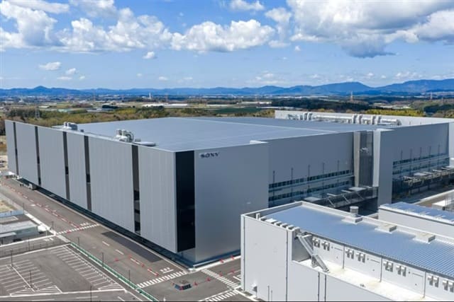
Sony Group and Taiwan Semiconductor Manufacturing Company are preparing to sink approximately $6.3 billion into a joint manufacturing facility dedicated to next-generation image sensors, according to Sony. The plant will rise in Kumamoto Prefecture on Japan's southern island of Kyushu, with the two companies aiming to begin commercial output by 2029.
The ownership split gives Sony roughly 60 percent of the venture and TSMC the remaining 40 percent, positioning the collaboration as a Sony-led operation that leverages TSMC's fabrication expertise. The investment, which translates to around one trillion yen, represents one of the larger cross-border semiconductor partnerships announced in Asia this year and underscores the strategic importance both companies place on imaging technology for smartphones, automotive systems, and industrial applications.
Kumamoto's Semiconductor Cluster
The choice of Kumamoto is deliberate. TSMC already operates a logic chip fabrication plant in the prefecture, which began production in late 2024 and supplies automotive and consumer electronics customers across Asia. Adding an image sensor line in the same region allows the partners to share infrastructure, logistics networks, and a skilled workforce trained in advanced semiconductor processes.
Japan has been courting leading-edge chipmakers with subsidies and streamlined permitting, part of a broader industrial policy to rebuild domestic semiconductor capacity after decades of decline. The government has committed billions in support to TSMC's existing Kumamoto fab, and industry observers expect similar backing for the image sensor venture, though neither Sony nor TSMC has disclosed the subsidy structure publicly.
For Sony, Kumamoto offers proximity to its existing sensor design centers and the chance to localize a critical supply chain that currently spans facilities in Nagasaki and overseas contract manufacturers. The company has long dominated the global image sensor market, holding more than 40 percent share by revenue, and views in-house manufacturing as essential to protecting its lead in pixel architecture and stacked sensor designs.
Why Image Sensors Matter Now
Image sensors sit at the heart of the smartphone camera revolution, but their role is expanding rapidly. Automotive makers are embedding multiple high-resolution sensors in vehicles for advanced driver assistance and future autonomy features. Industrial robotics, medical imaging, and augmented reality devices all demand sensors with higher dynamic range, lower power consumption, and faster readout speeds - specifications that push the boundaries of current manufacturing techniques.
Sony's existing sensor lines rely on mature process nodes and older equipment. The new facility is expected to employ cutting-edge lithography and stacking technologies that integrate logic circuits directly beneath the photodiode array, shrinking module size and improving signal processing. TSMC brings experience in advanced packaging and high-volume yield management, capabilities Sony can tap without building that expertise internally.
The partnership also reflects competitive pressure. Samsung has been investing heavily in its own sensor division, aiming to close the gap with Sony in premium smartphone and automotive segments. Chinese sensor makers, though still trailing in performance, are gaining share in mid-range devices. By locking in TSMC's manufacturing muscle, Sony aims to maintain its technology lead and secure capacity in a market where fab space is increasingly contested.
Timeline and Execution Risk
A 2029 production start leaves roughly four years for site preparation, clean-room construction, equipment installation, and process validation - a timeline that is ambitious but not unprecedented for greenfield semiconductor projects in Japan. TSMC's track record in Kumamoto, where it brought its first fab online faster than many analysts expected, provides some confidence, though image sensors introduce different technical challenges than the logic chips TSMC produces at scale.
Demand forecasting adds another layer of complexity. The smartphone market has plateaued in volume terms, and while automotive and industrial sensors are growing, those segments are smaller and more fragmented. Sony and TSMC will need to calibrate capacity carefully to avoid the boom-bust cycles that have plagued other semiconductor investments in recent years.
Still, the scale of the commitment signals both companies see image sensors as a durable growth category. For TSMC, the venture diversifies revenue beyond logic chips and deepens its strategic relationship with one of Japan's most influential electronics groups. For Sony, it secures manufacturing independence at a moment when supply chain resilience has become a boardroom priority across Asia.
RELATED STORIES
Asian Tech Stocks Surge as Weak US Jobs Data Dims Rate Hike Outlook
Cheng Wei-Lun · 4 min
Japan Embeds Cyber Defense in Air Force Systems as AI Threats Grow
Aiko Nakamura · 4 min

Tesla Expands Japan Delivery Network to Meet Rising EV Demand
Aiko Nakamura · 3 min

Rashi Peripherals and Restar Form Joint Venture to Expand Semiconductor Services in India
Priyanka V. Rao · 2 min
Spot something wrong? Email editor@briefasia.com. We log every correction publicly.