Technology · Dev
SK Hynix Commits $4.8 Billion to Fast-Track Advanced Packaging Plant in South Korea
The memory chipmaker is pouring capital into its Cheongju P&T7 facility while maintaining its broader KRW 19 trillion investment envelope, betting on surging AI-driven demand for high-bandwidth memory.
KEY TAKEAWAYS
- ·SK Hynix's board approved KRW 7.09 trillion for its P&T7 advanced packaging plant in Cheongju, South Korea, on July 22, 2026.
- ·The chipmaker is accelerating construction to capture AI-driven demand for high-bandwidth memory while keeping its total investment budget at KRW 19 trillion.
- ·Pilot production at P&T7 is expected in late 2027, with volume ramp planned for the first half of 2028.
Board Green-Lights Accelerated Construction
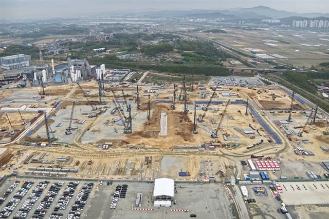
SK Hynix's board authorized approximately KRW 7.09 trillion in facility spending on July 22, directing the funds toward its P&T7 advanced packaging plant in Cheongju, South Korea. The allocation, equivalent to around $4.83 billion at current exchange rates, is designed to speed up construction timelines without expanding the company's overall capital commitment, which remains anchored at KRW 19 trillion.
The chipmaker broke ground on the P&T7 site on April 22, 2026. The latest capital infusion suggests management is prioritizing packaging capacity as global demand for high-bandwidth memory intensifies, particularly from hyperscale data center operators and AI accelerator manufacturers.
Why Packaging Matters in the AI Chip Race
Advanced packaging has emerged as a critical bottleneck in the semiconductor supply chain. Unlike traditional wire-bonding, modern packaging techniques stack memory dies vertically or arrange them side-by-side using through-silicon vias and micro-bumps, dramatically increasing data throughput between compute and memory. SK Hynix's HBM3E products, which rely on these methods, are already shipping to customers building large language model training clusters.
The Cheongju facility will house cleanroom space dedicated to these processes. By concentrating capital on P&T7, SK Hynix is betting that packaging capacity, rather than raw wafer fabrication, will determine market share in the high-margin AI segment over the next three years.
Capital Discipline Amid Expansion
The KRW 7.09 trillion figure represents a substantial slice of SK Hynix's standing KRW 19 trillion investment plan, yet the company has not revised that aggregate ceiling upward. This suggests the firm is reallocating funds from other projects or phasing spending more aggressively into the current and next fiscal year.
South Korean memory makers have historically operated on multi-year capital cycles, balancing investment with expected demand and price trends. SK Hynix's decision to accelerate P&T7 while holding the overall budget flat indicates confidence that near-term AI infrastructure buildout will absorb the additional capacity without triggering a supply glut.
Regional Context and Competition
South Korea's semiconductor ecosystem is under pressure to maintain its lead in memory technology as competitors in the United States and China expand domestic production. Washington has extended grants and low-cost loans to chipmakers willing to build on American soil, while Beijing continues to funnel capital into CXMT and other domestic DRAM producers despite export control headwinds.
SK Hynix's Cheongju investment reinforces South Korea's strategy of doubling down on advanced nodes and packaging, where process know-how and yield management remain significant moats. The country's chipmakers have also benefited from stable power supply and established supplier networks for specialty gases, photoresists, and inspection equipment, all of which are essential for high-volume cleanroom operations.
What Comes Next
The P&T7 facility is expected to begin pilot production in late 2027, with volume ramp planned for the first half of 2028. Timing will depend on equipment installation schedules and qualification runs with anchor customers. SK Hynix has not disclosed which specific products will initially run through the Cheongju line, but industry observers expect HBM4 variants and potentially co-packaged optics modules to feature prominently.
If demand for AI accelerators remains strong through 2027, the company may face pressure to expand cleanroom square footage further or retrofit older fabs for packaging duty. For now, management appears content to execute the existing roadmap and watch how the market absorbs capacity additions from Samsung and Micron, both of which have announced their own packaging expansions in recent quarters.
The Cheongju project also carries implications for South Korea's broader industrial policy. The government has offered tax incentives and streamlined permitting for semiconductor facilities deemed strategic, and P&T7 qualifies under those criteria. As global chip supply chains fragment along geopolitical lines, Seoul's ability to keep capital flowing into cutting-edge capacity will shape its position in the next wave of technology competition.
RELATED STORIES
Samsung Workers Plan Protest Over Pay Gap Between Chip and Device Units
Jun-ho Seo · 3 min
Memory Makers Gain Leverage as AI Server Costs Climb
Cheng Wei-Lun · 3 min
South Korean Chip Materials Suppliers Ride AI Boom to Profit Surge
Cheng Wei-Lun · 3 min
South Korea Taps Three Telecom Giants to Deliver Free AI Services Nationwide
Cheng Wei-Lun · 3 min
Spot something wrong? Email editor@briefasia.com. We log every correction publicly.