Technology · Dev
Shanghai Chipmaker AMIES Secures Volume Orders for 350nm Lithography System
The AST6200 stepper marks a strategic expansion for the Chinese equipment maker beyond its core advanced-packaging business, validated at a major compound-semiconductor facility.
KEY TAKEAWAYS
- ·Shanghai-based AMIES Technology secured repeat volume orders for its AST6200 350nm lithography stepper after process validation at a major Chinese compound-semiconductor manufacturer.
- ·The 350nm node remains critical for power devices, RF chips, and optoelectronics, segments where compound semiconductors like gallium nitride and silicon carbide dominate.
- ·Compound-semiconductor fabs offer a strategic entry point for domestic toolmakers due to lower volumes, specialized substrates, and reduced competition from hyperscale silicon foundries.
Domestic Tool Gains Traction in Compound Semiconductors
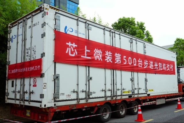
Shanghai-based AMIES Technology has landed repeat production orders for its AST6200 350nm stepper projection lithography system, marking the first major commercial validation of the domestically developed tool. The equipment passed process qualification at a prominent Chinese compound-semiconductor manufacturer, according to the company, extending AMIES's footprint beyond the advanced-packaging segment where it built its reputation.
The orders represent a strategic inflection for AMIES. While the Shanghai firm has long supplied packaging and back-end equipment to Chinese fabs, the AST6200 moves it into front-end lithography, a category dominated by ASML, Nikon, and Canon. The 350nm node sits well behind the leading edge, but it remains essential for power devices, radio-frequency chips, sensors, and optoelectronics, categories in which compound semiconductors like gallium nitride and silicon carbide play critical roles.
Why 350nm Still Matters
Lithography at the 350nm node is not cutting-edge by consumer-chip standards, yet it underpins a large swath of industrial and automotive electronics. Compound-semiconductor fabs, in particular, rely on mature nodes to manufacture high-voltage power transistors, LED drivers, and RF components for 5G infrastructure. These applications prioritize reliability, thermal performance, and cost over transistor density, making 350nm tools commercially viable decades after their introduction in mainstream logic.
For China, domestic lithography capability at any node carries strategic weight. Export controls introduced by the United States, the Netherlands, and Japan have restricted Chinese access to advanced lithography systems, including deep-ultraviolet and extreme-ultraviolet tools. While 350nm steppers fall outside the most sensitive categories, Beijing has pressed equipment makers to localize supply chains across the entire spectrum of semiconductor manufacturing.
AMIES's success in securing volume orders suggests that at least one major customer views the AST6200 as production-ready. Process validation in semiconductor manufacturing is rigorous, typically involving months of wafer testing, yield analysis, and reliability qualification. Repeat orders indicate that initial production runs met the customer's throughput, overlay accuracy, and defect-density requirements.
AMIES's Packaging Pedigree
AMIES built its business around advanced-packaging tools, a segment that has grown rapidly as chipmakers turn to 2.5D and 3D integration to maintain performance gains in the absence of easy transistor scaling. The company supplies lithography and inspection equipment for wafer-level packaging, flip-chip bonding, and through-silicon-via processes. These tools operate at geometries similar to or coarser than 350nm, giving AMIES relevant optical and mechanical engineering experience.
The AST6200 leverages that expertise but applies it to front-end wafer patterning, a different set of process requirements. Stepper lithography demands precise stage control, high-quality optics, and tight overlay budgets, especially when the tool must integrate into existing fab workflows alongside metrology and etch systems from other vendors. AMIES has not disclosed technical specifications for the AST6200, but industry observers note that 350nm steppers typically use mercury arc lamps and refractive optics, mature technologies that Chinese suppliers can source or manufacture domestically.
Compound Semiconductors as Beachhead
Compound-semiconductor fabs offer a logical entry point for domestic lithography tools. These facilities often operate at lower volumes than large logic or memory plants, reducing the pressure for maximum throughput. They also tend to use specialized substrates, sapphire, silicon carbide, or gallium arsenide, which require process recipes distinct from standard silicon. A Chinese equipment maker willing to work closely with customers on process development can carve out share more easily than in the hypercompetitive silicon foundry market.
China has invested heavily in compound semiconductors as part of its push for self-sufficiency in power electronics and RF devices. Domestic demand for gallium-nitride power chips has surged alongside electric-vehicle production and renewable-energy installations, both policy priorities in Beijing. If AMIES can demonstrate consistent performance in this segment, it may attract additional customers in adjacent markets, including MEMS sensors and photonics.
What Comes Next
The immediate question is scale. Repeat orders from one customer do not yet constitute a broad installed base, and AMIES will need to prove the AST6200's reliability across multiple fabs and process flows. Competing against established Japanese and European toolmakers will require not only matching technical specifications but also offering competitive service, spare-parts availability, and software support.
Longer term, AMIES's ambitions likely extend to finer geometries. China's equipment ecosystem has made incremental progress at 90nm and 65nm, with domestic scanners and steppers entering pilot production at select fabs. Moving from 350nm to sub-100nm involves significant engineering challenges, including shorter-wavelength light sources, more complex optics, and tighter process control, but the path is well understood. If AMIES can secure cash flow and technical feedback from the AST6200, it will have a foundation for iterating toward more advanced nodes.
For now, the AST6200 represents a modest but tangible step in China's semiconductor localization drive. The compound-semiconductor segment may not grab headlines the way leading-edge logic does, but it is large, growing, and strategically important. A domestic lithography tool that can meet production requirements in that segment is a building block, not a breakthrough, but building blocks matter when the goal is a self-reliant supply chain.
RELATED STORIES
China Unveils Immersion DUV Lithography System Amid Export Controls
Cheng Wei-Lun · 3 min

Cambricon Revenue Doubles as Chinese AI Chip Demand Outpaces Capacity
Cheng Wei-Lun · 3 min

Samsung Doubles BOE Panel Orders as Chinese Suppliers Tighten Grip on TV Display Market
Cheng Wei-Lun · 3 min
Seoul Warns Against Redistributing Chip Profits as China Investment Accelerates
Jun-ho Seo · 2 min
Spot something wrong? Email editor@briefasia.com. We log every correction publicly.