Technology · Dev
China Unveils Immersion DUV Lithography System Amid Export Controls
Homegrown equipment marks milestone in semiconductor self-sufficiency, though production viability remains years away
KEY TAKEAWAYS
- ·China has developed an immersion deep-ultraviolet lithography system, equipment essential for producing chips below 90 nanometers and previously restricted by US export controls.
- ·Industry experts warn that commercial viability depends on wafer throughput, defect rates, and yield performance, challenges that typically require years of refinement and process validation.
- ·If the system reaches production scale, it could reduce Chinese reliance on imported equipment and complicate efforts to maintain technology chokepoints in the Asian semiconductor supply chain.
A Technical Milestone in Beijing's Chip Push
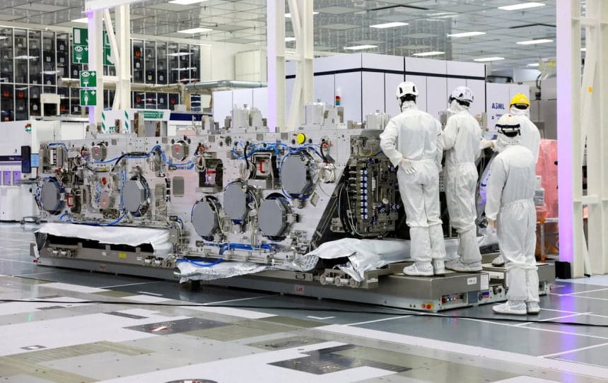
China has unveiled a domestically developed immersion deep-ultraviolet lithography system, a piece of equipment central to advanced semiconductor manufacturing that Washington has worked to keep out of Beijing's hands. The announcement arrives as Chinese chipmakers face tightening restrictions on access to Western fabrication technology, pushing the country to accelerate indigenous development of critical tooling.
Immersion DUV lithography uses liquid to increase the resolution of light patterns etched onto silicon wafers, enabling production of chips at nodes below 90 nanometers. The technology sits one generation behind extreme ultraviolet lithography but remains essential for producing a wide range of semiconductors, from automotive controllers to consumer electronics processors.
Beijing has poured resources into closing the gap in lithography, the most capital-intensive and technically complex segment of the semiconductor supply chain. ASML, the Dutch equipment giant that dominates the global market, has been barred from shipping its most advanced systems to China since 2019, with restrictions expanding to cover additional DUV models in subsequent years.
The Yield Question
Industry observers in Seoul and Taipei emphasize that demonstrating a working prototype and operating a system at commercial scale are fundamentally different challenges. Lithography equipment must maintain nanometer-level precision across millions of exposures, process hundreds of wafers per day, and deliver yields high enough to justify the capital expenditure, which for a single machine can exceed one hundred million dollars.
Wafer throughput and defect rates determine whether a lithography tool is economically viable. Even minor deviations in optical alignment, stage movement, or environmental control can cascade into yield losses that render a fabrication line unprofitable. Established suppliers like ASML and Nikon refined their platforms over decades, accumulating process knowledge that extends far beyond the base technical specifications.
China's semiconductor equipment industry has made measurable progress in etching, deposition, and inspection tools, but lithography remains the most stubborn bottleneck. Shanghai Micro Electronics Equipment, the country's leading lithography vendor, has been working on 28-nanometer-capable DUV systems for years, though volume adoption by major fabs has been limited.
Strategic Implications for Asia's Chip Ecosystem
The emergence of a Chinese immersion DUV system carries implications for the broader Asian semiconductor landscape. South Korea and Taiwan anchor the region's advanced fabrication capacity, with Samsung and TSMC operating the most sophisticated fabs outside the United States. Both companies rely on ASML lithography and have benefited from export restrictions that limit competition from Chinese foundries at leading-edge nodes.
If Beijing can field lithography equipment capable of supporting mature-node production at scale, it would reduce reliance on imports and complicate efforts by Washington and its allies to maintain technology chokepoints. Chinese chipmakers currently depend on stockpiled or smuggled equipment to sustain production at nodes between 14 and 28 nanometers, a segment that accounts for the majority of global semiconductor demand by volume.
Yet the path from prototype to production-ready tool is measured in years, not quarters. Lithography systems require extensive qualification by chipmakers, who must validate performance across multiple process flows and product families before committing to volume manufacturing. Any instability in throughput or yield during this phase can delay adoption indefinitely.
What Comes Next
The timeline for commercial deployment hinges on how quickly Chinese equipment makers can iterate on early designs, build out supply chains for precision optics and motion control components, and secure customer commitments from domestic fabs. Beijing has demonstrated willingness to subsidize deployment of indigenous equipment even when performance lags foreign alternatives, but the capital intensity of semiconductor manufacturing imposes hard limits on how much inefficiency the industry can absorb.
For now, the announcement underscores the durability of China's drive toward chip self-sufficiency, even as it highlights the distance still to be covered. Whether the system can transition from technical achievement to manufacturing workhorse will shape the competitive dynamics of Asia's semiconductor industry for the next decade.
RELATED STORIES

SK Hynix Eyes Stake Sale in $3 Billion China Packaging Facility
Cheng Wei-Lun · 2 min

Asia's Memory Makers Shift Focus as DRAM Margins Challenge HBM Dominance
Cheng Wei-Lun · 4 min

GlobalFoundries Posts Stronger Second-Quarter Results on AI Optics Demand
Cheng Wei-Lun · 4 min

Beijing's AI Bar Offers Free DeepSeek Access as Price Wars Reshape Global Market
Cheng Wei-Lun · 3 min
Spot something wrong? Email editor@briefasia.com. We log every correction publicly.