Technology · AI
Semiconductor Battle Moves Beyond Chip Scaling as AI Demands Reshape Industry
Advanced packaging and system integration emerge as new competitive fronts while transistor miniaturization slows
KEY TAKEAWAYS
- ·Semiconductor competition is shifting from transistor scaling to system-level integration and advanced packaging as AI bandwidth demands outpace traditional process-node progress.
- ·ASE Technology Holding raised capital spending 23.5 percent to $10.5 billion, with 70 percent earmarked for leading-edge advanced packaging capacity expansion.
- ·Hardware infrastructure is becoming the primary bottleneck in AI deployment, driving moves toward panel-level packaging and optical interconnects to manage power and latency constraints.
The New Competitive Front
The semiconductor industry's decades-long focus on shrinking transistors is giving way to a broader battle over system architecture, advanced packaging, and integration capabilities. AI workloads are forcing chipmakers and packaging houses to rethink how components connect, communicate, and manage power at scale.
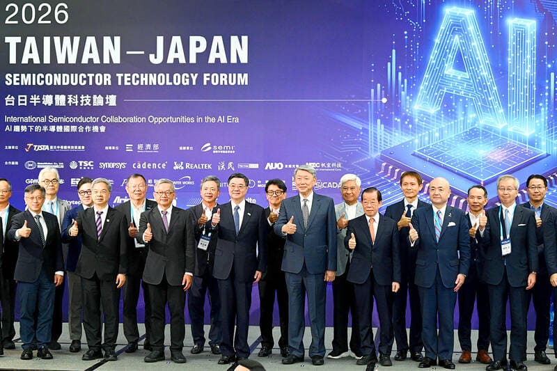
Tsai Hann-huei, deputy director-general at Taiwan Semiconductor Research Institute, told a technology forum in Taipei that process-node progress is decelerating while bandwidth requirements surge. Leadership in the next phase will depend on system-level co-optimization rather than transistor density alone, according to TSRI.
The shift reflects a practical constraint: AI models are growing faster than chip performance can keep pace using traditional scaling methods. Applications ranging from autonomous vehicles to humanoid robots now require chips that combine computing, sensing, power management, and connectivity in single packages.
Hardware Becomes the Constraint
Physical infrastructure is emerging as the primary bottleneck in AI deployment. Dinos Huang, senior director of corporate research at ASE Technology Holding, said the rapid expansion of AI models is placing unprecedented stress on the systems that run them.
Bandwidth and computing power demands are colliding with challenges in power consumption, latency, thermal management, and mechanical stability. ASE, the world's largest packaging and testing services provider, is responding by shifting from wafer-level to panel-level packaging. The larger format improves material utilization and accommodates the growing die sizes of AI processors.
The company is also pursuing optical interconnects to replace electrical transmission between chips and systems. The technology enables higher data rates while cutting energy use, a critical trade-off as data centers grapple with power constraints.
Integration Complexity Rises
Heterogeneous integration, which combines different chip types and functions in a single package, is becoming standard practice for high-performance systems. But the approach introduces new engineering challenges at the intersection of thermal, electrical, optical, and mechanical domains.
TSRI operates a die-level heterogeneous integration and verification platform to help designers prototype next-generation systems. The institute is working with Japanese partners on three-dimensional integration, advanced packaging, quantum computing, power devices, and materials analysis.
Large-scale testing and coordination across the semiconductor supply chain remain obstacles. Tsai emphasized that overcoming these barriers will require sustained collaboration among industry, academia, and research institutions.
Materials and Equipment Under Pressure
The packaging industry must develop new equipment, low-loss materials, and heat-resistant substrates to support the next wave of AI chips. Inspection, testing, and smart manufacturing capabilities also need upgrading to handle the complexity of heterogeneous designs.
Silicon photonics, which uses light instead of electrical signals to move data, faces particular challenges. The technology promises dramatic improvements in bandwidth and energy efficiency, but integrating optical components with silicon chips at scale requires advances in materials science and manufacturing precision.
Regional Collaboration in Focus
The forum, organized by the Taiwan-Japan Semiconductor Technology Association, centered on bilateral opportunities in AI-era semiconductor development. Taiwan's strength in advanced manufacturing and packaging complements Japan's materials and equipment expertise, creating potential synergies as both regions seek to secure positions in AI supply chains.
ASE raised its capital expenditure for the year to $10.5 billion, a 23.5 percent increase from its earlier budget, with about 70 percent allocated to capacity expansion. The company expects revenue from leading-edge advanced packaging technology to exceed $3.5 billion this year.
The competitive dynamics reshaping the industry reflect a broader reality: AI is pushing semiconductor design and manufacturing into domains where traditional metrics like transistor count matter less than system-level performance, energy efficiency, and integration sophistication. Companies that master these disciplines will define the next phase of the industry.
RELATED STORIES

Taiwan's AI Supply Chain Posts Record $89.7 Billion in August Revenue
Jun-ho Seo · 2 min
Tokyo Summit Pushes Trilateral Tech Alliance Among Taiwan, Japan, and US
Cheng Wei-Lun · 3 min
AI Demand Tightens Memory Markets as HBM4 Production Strains Supply
Cheng Wei-Lun · 3 min

Manila's Chip Industry Still Stalled in Assembly While Taipei Built Fabs
Priyanka V. Rao · 4 min
Spot something wrong? Email editor@briefasia.com. We log every correction publicly.