Technology · Dev
Samsung Introduces zHBM Concept for Next-Generation AI Computing
The Korean chipmaker's new memory architecture aims to deliver eight times the performance of upcoming HBM5 standard
KEY TAKEAWAYS
- ·Samsung Electronics introduced zHBM concept models at a California conference, targeting performance eight times greater than the upcoming HBM5 memory standard.
- ·The new architecture addresses escalating AI workload demands through fundamental design changes rather than incremental improvements to existing high-bandwidth memory.
- ·Samsung's early disclosure reflects both technical ambition and strategic pressure from SK hynix's current leadership in HBM3E production and customer partnerships.
A New Memory Frontier
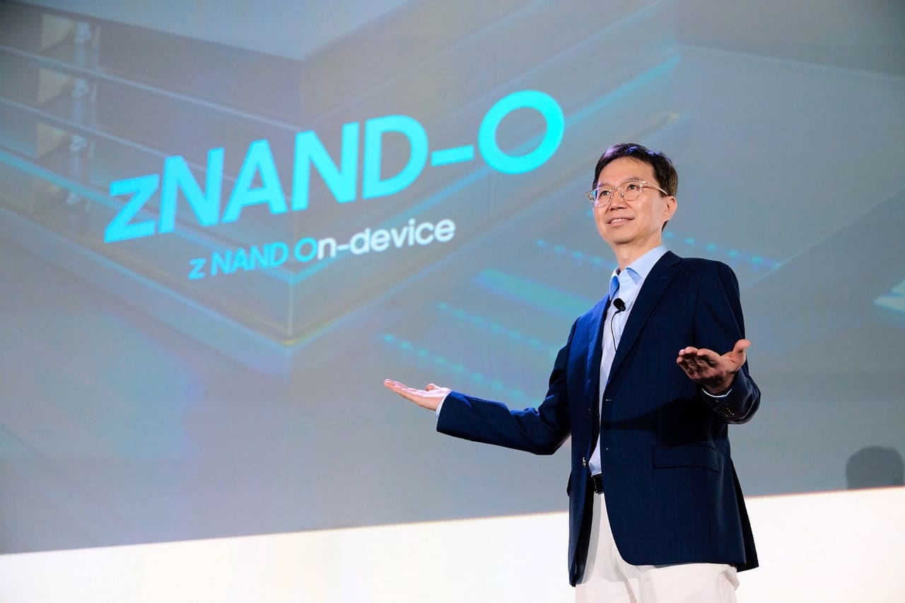
Samsung Electronics unveiled concept models of zHBM this week, introducing what it describes as a fundamentally new memory architecture for artificial intelligence computing. The technology targets performance roughly eight times greater than HBM5, the next iteration of high-bandwidth memory expected to reach production in the coming years.
The company presented the technology at the Future of Memory and Storage 2026 conference in Santa Clara, California, marking the first public demonstration of this architectural approach. Samsung positions zHBM as a response to escalating bandwidth and capacity demands from AI training and inference workloads that continue to outpace incremental improvements in existing memory standards.
Breaking the HBM Roadmap
Traditional high-bandwidth memory has followed a predictable evolution, with each generation delivering incremental gains in bandwidth, capacity, and energy efficiency through denser stacking and faster interfaces. HBM3 currently powers many AI accelerators, while HBM4 samples are circulating among hyperscale customers. HBM5 remains in the specification phase, with production not anticipated until late 2027 or 2028.
Samsung's zHBM concept represents a departure from this linear progression. Rather than simply adding more layers or increasing clock speeds, the architecture rethinks how memory dies communicate with processing units and with each other. The eight-fold performance claim suggests a combination of higher bandwidth per pin, greater parallelism, and potentially new signaling technologies that reduce latency and power consumption per bit transferred.
The company has not disclosed technical specifics such as stack height, interface width, data rates, or power envelopes. Industry observers note that achieving an eight-fold improvement over HBM5 without proportional increases in power or cost would require innovations across multiple layers of the design, from die-to-die interconnects to thermal management.
The Asia Memory Race
Samsung's announcement arrives amid intensifying competition in the memory sector across Northeast Asia. SK hynix has captured significant market share in HBM3E, the current leading-edge standard, through close partnerships with Nvidia and other AI accelerator designers. Micron Technology, though headquartered in the United States, manufactures much of its HBM in Taiwan and Japan, further concentrating production in the region.
For Samsung, demonstrating leadership in next-generation memory architectures serves both technical and strategic purposes. The company has historically led DRAM innovation but has faced execution challenges in the current HBM cycle, including yield issues and delayed qualification timelines with key customers. A successful zHBM program could reestablish Samsung's position as the technology pacesetter and provide leverage in negotiations with hyperscale cloud providers and AI hardware companies planning roadmaps beyond 2028.
China's memory ambitions add another dimension to the competitive landscape. Although Chinese firms remain several generations behind in HBM production, state-backed investment continues to flow into domestic memory capabilities. Any architectural shift that resets the technology baseline could theoretically narrow the gap, making early leadership in new standards a priority for incumbents.
Concept to Production
Samsung characterized the zHBM presentation as a concept demonstration rather than a product announcement. The path from laboratory prototype to high-volume manufacturing typically spans three to five years for advanced memory, requiring extensive co-design with processor architects, validation across workloads, and ecosystem support from software and system vendors.
The conference venue, Santa Clara, places Samsung in proximity to many of the AI hardware designers and hyperscale data center operators who will ultimately determine whether zHBM becomes a commercial standard or remains a research exercise. These customers are already collaborating with memory makers on HBM4 and beginning early discussions around HBM5 requirements. Introducing a parallel track with zHBM allows Samsung to gauge interest and gather feedback while continuing to execute on the established roadmap.
Timing will prove critical. If HBM5 meets the performance and efficiency targets AI workloads demand when it reaches production, the industry may see limited incentive to adopt a more radical architecture. Conversely, if AI model scaling continues to outstrip memory capabilities, zHBM or similar approaches could become necessary rather than optional. Samsung's early disclosure suggests confidence that the latter scenario is more likely, and that staking a claim to the post-HBM5 architecture now will yield strategic advantage in the years ahead.
RELATED STORIES
Samsung and SK Hynix Turn Down KEPCO's Multibillion-Dollar Prepayment Demand
Cheng Wei-Lun · 4 min

South Korea Records Highest September Export Start on Semiconductor Demand
Tran Quoc Bao · 3 min
SK Hynix May Fast-Track Gwangju Fab Investment Alongside Yongin Expansion
Jun-ho Seo · 3 min
Memory Makers Gain Leverage as AI Server Costs Climb
Cheng Wei-Lun · 3 min
Spot something wrong? Email editor@briefasia.com. We log every correction publicly.