Technology · Dev
HKC Bets $590 Million on Chip Packaging to Break Free of LCD Volatility
The world's third-largest LCD panel maker joins BOE and other Chinese display manufacturers in pivoting upstream toward semiconductors as the industry seeks revenue diversification.
KEY TAKEAWAYS
- ·HKC plans to invest CNY4 billion (approximately $590 million) in a 12-inch chip packaging and testing facility, marking a strategic shift from cyclical LCD panel manufacturing to higher-margin semiconductor services.
- ·The move follows a broader trend among Chinese display makers, including BOE, seeking to diversify into semiconductors as advanced packaging capacity becomes a critical bottleneck in AI accelerator and chiplet production.
- ·HKC will compete in a crowded market dominated by Taiwanese and South Korean players with decades of experience, though China's policy push for supply chain localization and surging domestic demand offer growth potential.
Display Giant Pivots to Semiconductors
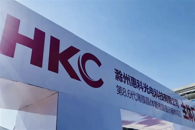
HKC, currently ranked as the world's third-largest supplier of LCD panels, announced plans to invest CNY4 billion (approximately $590 million) in a new 12-inch chip packaging and testing facility. The move signals a strategic pivot away from the cyclical and increasingly commoditized LCD business toward higher-margin semiconductor services.
The investment places HKC alongside BOE and other major Chinese display manufacturers pursuing vertical integration into the semiconductor supply chain. For years, panel makers have weathered brutal price cycles driven by overcapacity and sluggish demand, prompting executives across the sector to explore adjacent markets with more stable returns.
Why Packaging Matters Now
Advanced chip packaging has emerged as a critical bottleneck in the semiconductor industry, particularly as chipmakers pursue chiplet architectures and heterogeneous integration to sustain performance gains beyond traditional scaling. The technology stacks multiple dies or chiplets into a single package, enabling higher bandwidth, lower power consumption, and better thermal management than conventional wire-bonding methods.
Demand for advanced packaging capacity has surged in tandem with AI accelerator production, where high-bandwidth memory and logic dies must be tightly integrated. Taiwan's backend houses have reported multi-quarter order backlogs, and leading foundries including TSMC have announced billions in packaging capex to support customers racing to deploy next-generation data center chips.
HKC's entry reflects China's broader ambition to build self-sufficient semiconductor capabilities across the stack, from materials and equipment to design, fabrication, and now packaging. While the country has made strides in trailing-edge logic and memory, advanced packaging remains a strategic gap, with most cutting-edge capacity concentrated in Taiwan, South Korea, and pockets of Southeast Asia.
The Display-to-Chip Playbook
HKC is not alone in this pivot. BOE, the world's largest LCD and OLED panel maker, has quietly expanded into semiconductor materials, driver ICs, and packaging over the past five years. The rationale is straightforward: display fabs already operate cleanrooms, employ similar lithography and deposition processes, and maintain relationships with equipment vendors that overlap heavily with semiconductor toolmakers.
Packaging lines require lower capital intensity than leading-edge logic fabs and face less stringent export control scrutiny, making them an attractive entry point for companies seeking to diversify without triggering geopolitical friction. A 12-inch packaging line typically costs a fraction of a comparable logic fab, yet can command gross margins in the mid-20s to low-30s range when running at utilization, well above the single-digit margins that have plagued the LCD industry during downturns.
HKC's facility will focus on 12-inch wafer-level packaging and testing, positioning the company to serve both domestic fabless chip designers and integrated device manufacturers looking to localize their supply chains. The timeline for volume production has not been disclosed, though industry observers expect initial output by late 2027 or early 2028, assuming equipment delivery and qualification proceed on schedule.
Risks and Realities
The strategy carries execution risk. Advanced packaging demands process know-how distinct from display manufacturing, particularly in areas like through-silicon vias, microbumping, and thermal interface materials. Yield ramp-ups can take years, and customers in the semiconductor industry have long memories when it comes to quality escapes or delivery failures.
Moreover, the market HKC is entering is already crowded. Established players in Taiwan and South Korea have decades of institutional knowledge, tight relationships with hyperscale customers, and proven track records in high-volume production. Chinese packaging houses such as JCET and Tongfu have also been expanding aggressively, supported by state subsidies and local customer mandates.
Still, the sheer scale of anticipated demand and Beijing's policy push for supply chain localization offer a tailwind. If HKC can secure anchor customers among China's fast-growing fabless sector and demonstrate competitive cycle times and yields, the investment may prove a durable hedge against the LCD cycle's next downturn.
What Comes Next
Industry watchers will monitor HKC's progress on equipment installation, talent acquisition, and customer engagement over the coming quarters. The company's ability to attract experienced packaging engineers, many of whom are currently employed by Taiwanese and South Korean rivals, will be a key indicator of the project's viability.
For the broader display industry, HKC's move underscores a structural shift: panel making alone no longer offers the margins or growth trajectories that investors and management teams demand. Diversification into semiconductors, whether through packaging, materials, or component supply, has become the prevailing playbook for survival in an era of persistent oversupply and geopolitical realignment.
RELATED STORIES
JCET Eyes $968 Million to Scale AI Packaging Lines
Tran Quoc Bao · 3 min
China's Chip Makers Split Three Ways Beneath the Revenue Growth
Tran Quoc Bao · 3 min
Hong Kong Debuts Robot-Run Convenience Store in Commercial Automation Push
Cheng Wei-Lun · 3 min

China Scrubs 5.6 Million AI-Generated Posts in Platform Cleanup
Cheng Wei-Lun · 3 min
Spot something wrong? Email editor@briefasia.com. We log every correction publicly.