Technology · Products
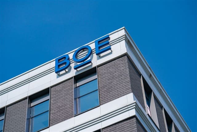
BOE Pushes Into Chip Manufacturing as China Extends Display Advantage
Beijing-backed panel leader advances glass substrates and prepares 12-inch wafer fab for production amid tightening US export controls
KEY TAKEAWAYS
- ·BOE Technology is preparing a 12-inch wafer fab for mass production in the second half of 2026, targeting mature-node chips and display driver ICs.
- ·The expansion leverages China's government-backed display panel expertise to enter semiconductor manufacturing, adding competitive pressure on South Korean chip and panel makers.
- ·Glass substrate development for advanced packaging represents a strategic technology area not yet covered by US export controls, enabling performance gains without cutting-edge process nodes.
Display Giants Turn Chipmakers
China's largest display panel manufacturer is crossing into semiconductor territory. BOE Technology has begun advancing glass substrate development and is preparing a 12-inch wafer fabrication facility for mass production in the second half of 2026, according to industry sources.
The move represents a strategic pivot for Chinese display makers, who are now channeling years of government-supported panel technology development into chip manufacturing. The timing coincides with Washington's expanding semiconductor export restrictions, which have pushed Beijing to accelerate domestic production capacity across the chip supply chain.
Strategic Leverage from Display Dominance
BOE's entry into chip production draws directly on technical capabilities developed through China's display panel industry, where the country now commands global market share. Glass substrate technology, central to advanced semiconductor packaging, shares significant overlap with the precision materials engineering required for LCD and OLED panel production.
The company's planned 12-inch wafer fab will target mature-node chip production, a segment critical to automotive electronics, industrial equipment, and consumer devices. While trailing-edge by leading foundry standards, these chips remain essential across manufacturing sectors and represent a gap in China's current domestic supply.
Industry analysts note that BOE and other Chinese panel makers accumulated substantial process expertise over the past decade, supported by multi-billion-dollar government subsidies and technology partnerships. That foundation now provides a platform for vertical integration into semiconductors, reducing reliance on foreign chip suppliers and creating new revenue streams as display panel margins compress globally.
Pressure on South Korean Industry
The expansion places additional competitive strain on South Korea's chip and display sectors, which face challenges on multiple fronts. Samsung Electronics and SK hynix dominate memory chip production but have seen Chinese competitors close the gap in mature-node logic chips and display driver ICs.
South Korea's panel industry, led by Samsung Display and LG Display, already contends with aggressive pricing from Chinese rivals. BOE's semiconductor push threatens to erode another advantage: integrated supply chains that combine panel and chip production under single corporate umbrellas.
Seoul has responded with its own subsidy programs, including the K-Chips Act, designed to shore up domestic semiconductor competitiveness. But China's scale and state backing present formidable obstacles. Beijing's support for strategic industries extends beyond direct subsidies to preferential financing, land grants, and coordinated procurement from state-owned enterprises.
Technology Transfer and Export Controls
BOE's chip ambitions also highlight ongoing debates over technology transfer and export control effectiveness. US restrictions on advanced chipmaking equipment sales to China aim to limit progress in cutting-edge nodes below 14 nanometers. Mature-node production, however, remains largely unrestricted, and Chinese firms have doubled down on capacity expansion in that segment.
Glass substrate technology for advanced packaging, which BOE is developing, occupies a gray zone. While not subject to current export controls, it enables performance improvements in chip design that partially offset limitations in process node advancement. The substrate approach allows multiple chiplets to be integrated on a single package, improving performance and reducing costs.
Washington has signaled interest in tightening controls on packaging and substrate technologies, but implementation remains complex. Allied coordination with Japan, South Korea, and the Netherlands is essential for effective enforcement, and each government balances security concerns against commercial interests.
Regional Implications
The broader shift of Chinese display makers into semiconductors carries implications across East Asia. Taiwan's foundries, particularly TSMC, remain insulated by their leadership in advanced nodes, but face potential long-term pressure if Chinese firms achieve breakthroughs in packaging and design.
Japan's equipment and materials suppliers occupy a delicate position, serving both Chinese and South Korean customers while navigating export restrictions. Tokyo has aligned with US controls on extreme ultraviolet lithography equipment but maintains commercial relationships with Chinese chipmakers in less restricted categories.
Southeast Asian nations, meanwhile, are positioning themselves as neutral assembly and testing hubs, attracting investment from Chinese, South Korean, and Taiwanese firms seeking to diversify supply chains. Vietnam and Malaysia have seen significant inflows in semiconductor backend operations over the past two years.
Production Timeline and Market Impact
BOE's 12-inch fab is expected to begin trial production in the third quarter of 2026, with volume manufacturing ramping through year-end. Initial output will focus on display driver ICs and power management chips, segments where the company can leverage existing customer relationships in consumer electronics.
The glass substrate initiative targets commercialization over a longer horizon, with pilot production anticipated in 2027. Successful development would position BOE as a supplier to both domestic and international chip designers seeking alternatives to established substrate manufacturers in Japan and Taiwan.
Market analysts caution that execution risks remain substantial. Semiconductor manufacturing requires precision and yield management beyond panel production, and BOE will compete against established foundries with decades of process refinement. Capital intensity is also significantly higher, with a single 12-inch fab requiring multi-billion-dollar investment.
Nonetheless, the strategic direction is clear. China's display industry, having achieved scale and technical competency, is leveraging that foundation to build semiconductor capacity. The move underscores Beijing's commitment to self-sufficiency in critical technologies and signals intensifying competition across Asia's electronics supply chains.
RELATED STORIES

Sharpa Secures $668 Million at $3.3 Billion Valuation in Tech Giant-Backed Round
Cheng Wei-Lun · 2 min

China Scrubs 5.6 Million AI-Generated Posts in Platform Cleanup
Cheng Wei-Lun · 3 min
China's Chip Makers Split Three Ways Beneath the Revenue Growth
Tran Quoc Bao · 3 min
JCET Eyes $968 Million to Scale AI Packaging Lines
Tran Quoc Bao · 3 min
Spot something wrong? Email editor@briefasia.com. We log every correction publicly.