Finance · Deals
TSMC and Sony Form $1.77 Billion Image Sensor Venture in Japan
The chipmaker will invest in Advanced Vision Semiconductor Manufacturing, targeting 2029 production start for next-generation smartphone sensors in Kumamoto
KEY TAKEAWAYS
- ·TSMC is investing ¥282 billion in a joint venture with Sony Semiconductor Solutions to manufacture next-generation smartphone image sensors in Kumamoto Prefecture, with production starting in 2029.
- ·Sony will contribute ¥465 billion in cash and assets to Advanced Vision Semiconductor Manufacturing, making it the majority investor with Japanese government financial backing.
- ·TSMC's board separately approved $29.44 billion in capital expenditures for advanced node capacity and new fabrication facilities, alongside a second-quarter dividend of NT$7 per share.
Chipmaker Doubles Down on Japan Expansion
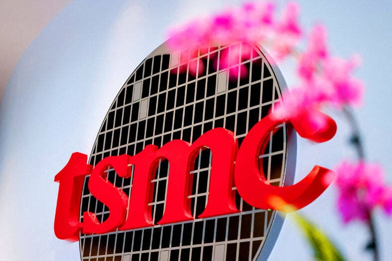
TSMC's board of directors has greenlit an investment of ¥282 billion ($1.77 billion) to establish a joint venture with Sony Semiconductor Solutions Corp, according to the company. The partnership will focus on developing and manufacturing next-generation image sensors for smartphones at a facility in Koshi City, Kumamoto Prefecture.
The new entity, Advanced Vision Semiconductor Manufacturing Corp, is expected to begin volume production in 2029. Sony Semiconductor will contribute ¥465 billion through a combination of cash and existing assets, making it the majority investor in the venture.
Capital contributions from both parties will be deployed in phases, contingent on market demand and broader economic conditions. The Japanese government is providing financial support for the project, though specific subsidy amounts were not disclosed.
The transaction remains subject to regulatory approval before it can be finalized.
Strategic Positioning in Image Sensor Market
The partnership positions TSMC deeper into the specialized image sensor market, a segment where Sony already commands significant share in smartphone camera components. By combining TSMC's advanced manufacturing capabilities with Sony's sensor design expertise, the venture aims to capture demand for higher-resolution and AI-enhanced imaging systems in mobile devices.
Kumamoto Prefecture has emerged as a focal point for semiconductor investment in Japan, driven by government incentives aimed at securing domestic chip supply chains. TSMC already operates a fabrication facility in the region, which began construction in 2021 and is expected to start production later this year.
The image sensor joint venture represents a distinct strategic bet from TSMC's existing Kumamoto operations, which focus on logic chips for automotive and industrial applications. Smartphone image sensors require different process technologies and have separate customer bases, primarily handset manufacturers seeking differentiated camera performance.
Aggressive Capital Deployment
Separately, TSMC's board approved capital appropriations totaling $29.44 billion to expand capacity in advanced nodes and packaging technologies, as well as to construct new fabrication facilities. The investment underscores the chipmaker's commitment to maintaining its lead in cutting-edge process technology amid intensifying competition from Samsung and Intel.
The board also declared a second-quarter cash dividend of NT$7 per share, matching the record payout from the first quarter. The distribution represents a 25.69 percent payout ratio based on earnings of NT$27.25 per share during the period.
TSMC's aggressive capital spending reflects sustained demand for advanced chips across data center, automotive, and mobile applications. The company has signaled that capacity additions will focus on nodes below 5 nanometers and advanced packaging solutions, both critical for AI accelerators and high-performance computing systems.
Regional Implications
The Sony partnership extends TSMC's operational footprint in Japan at a time when Tokyo is actively courting foreign semiconductor investment to rebuild domestic chip manufacturing capacity. Japan's economic security strategy prioritizes reducing reliance on offshore production for critical components, including image sensors used in defense and surveillance systems.
For Sony, the venture provides access to TSMC's manufacturing scale and process expertise without requiring the capital-intensive buildout of wholly owned fabs. The arrangement mirrors partnerships Sony has pursued in other semiconductor segments, where it retains design control while outsourcing fabrication to specialist foundries.
The 2029 production timeline suggests both companies anticipate continued growth in smartphone imaging capabilities, despite recent market saturation in handset sales. Industry analysts expect demand for advanced sensors to be driven by computational photography, augmented reality features, and AI-driven image processing, all of which require more sophisticated semiconductor architectures.
The Kumamoto site selection also positions the venture near TSMC's existing infrastructure, enabling shared logistics, workforce development, and supply chain coordination across multiple facilities in the region.
RELATED STORIES
TSMC and Sony Plan $6.3 Billion Sensor Factory in Japan
Cheng Wei-Lun · 3 min
Sony and TSMC Plot $6.3 Billion Image Sensor Plant in Southern Japan
Cheng Wei-Lun · 3 min
Asian Tech Stocks Surge as Weak US Jobs Data Dims Rate Hike Outlook
Cheng Wei-Lun · 4 min

Franklin Templeton Restructures Leadership With Two Senior Appointments
Priyanka V. Rao · 4 min
Spot something wrong? Email editor@briefasia.com. We log every correction publicly.