Technology · Dev
SK Hynix Opens San Jose Design Hub for Custom 3D DRAM
South Korean memory giant recruits US engineers to co-design stacked DRAM-on-logic architectures with American chip clients, pushing custom memory beyond data centers into on-device AI.
KEY TAKEAWAYS
- ·SK Hynix is recruiting engineers in San Jose to co-design 3D stacked DRAM-on-logic architectures with US chip companies for on-device AI applications.
- ·The initiative extends SK Hynix's custom memory strategy beyond high-bandwidth memory for data centers into mobile, automotive, and edge inference processors.
- ·Co-located engineering allows faster collaboration on interface protocols, thermal design, and manufacturing splits between memory supplier and chip designer.
Silicon Valley Footprint
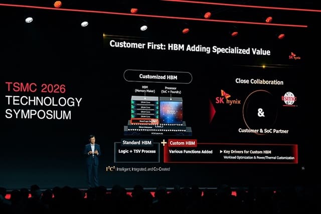
SK Hynix is building an engineering presence in San Jose, California, to collaborate with American semiconductor companies on custom three-dimensional memory architectures. The recruitment drive targets design talent capable of integrating stacked DRAM directly onto logic chips, a configuration distinct from the high-bandwidth memory modules the Korean firm already ships to hyperscale data centers.
The move signals a strategic bet that future AI workloads will demand memory solutions tailored to specific processor designs, rather than off-the-shelf commodity modules. By stationing engineers near clients in Silicon Valley, SK Hynix aims to shorten design cycles and capture socket wins in mobile processors, edge inference accelerators, and automotive compute platforms where power and latency matter more than raw bandwidth.
Beyond High-Bandwidth Memory
SK Hynix has built a dominant position in HBM, the stacked memory used in Nvidia and AMD data-center GPUs. That business, however, serves a concentrated customer base with largely standardized requirements. The San Jose initiative targets a broader and more fragmented market: chip designers building application-specific processors for smartphones, drones, industrial robots, and vehicles.
Three-dimensional DRAM-on-logic architectures place memory dies vertically atop or beneath compute silicon, connected by dense through-silicon vias or hybrid bonding. The approach cuts data travel distance, lowers power consumption, and enables smaller form factors. These advantages matter most in battery-powered or space-constrained devices, where traditional memory modules mounted beside the processor impose penalties.
Co-design is central to the model. Unlike standard memory products defined by JEDEC specifications, stacked memory-logic integration requires joint decisions on interface protocols, thermal management, and manufacturing splits between the memory supplier and the chip designer. Locating engineers in San Jose allows SK Hynix to participate in architecture discussions months before tape-out, rather than responding to finished designs.
The On-Device AI Catalyst
Demand for on-device AI inference is reshaping memory economics. Large language models and computer-vision networks once confined to cloud servers are migrating to endpoints, driven by latency, privacy, and connectivity constraints. Running these models locally demands high memory capacity and bandwidth within strict power budgets, a combination difficult to achieve with conventional LPDDR or DDR modules soldered onto a board.
Stacked memory architectures compress the physical distance between compute and storage, enabling higher data rates per watt. For a smartphone running real-time translation or a security camera analyzing video frames, the energy savings translate directly into longer battery life or lower operating cost. Automotive systems, which must process sensor fusion and path planning in real time, face similar trade-offs.
Several US chip designers have already announced processors with integrated or closely stacked memory. Apple's M-series and A-series chips use package-on-package DRAM. Qualcomm and MediaTek are exploring advanced packaging for their mobile platforms. Tesla's custom inference chip reportedly employs stacked SRAM. Each implementation requires negotiation with memory suppliers over capacity, bandwidth, and manufacturing responsibility, creating an opening for SK Hynix to differentiate through engineering support rather than price alone.
Competitive Landscape
Samsung and Micron, SK Hynix's principal rivals, are pursuing similar strategies. Samsung operates advanced-packaging facilities in South Korea and has co-developed memory solutions with Nvidia and Google. Micron maintains design centers in California and has partnered with automotive chipmakers on custom LPDDR and GDDR modules. The race is less about who can manufacture the densest or fastest memory, and more about who can embed their technology into the next generation of processors before architectures solidify.
Taiwanese and Chinese memory startups, though smaller, are also courting fabless designers with promises of flexible terms and faster prototyping. CXMT and Nanya have announced partnerships with domestic chip companies in China, where export controls on advanced US semiconductors have intensified demand for indigenous alternatives. SK Hynix's San Jose hub positions it to defend share among American customers even as the memory market fragments along geopolitical lines.
What Comes Next
The San Jose hiring is an early indicator, not a finished strategy. SK Hynix has not disclosed headcount targets, timeline, or which customers it is already working with. The company's chief design officer discussed memory-logic integration publicly at a recent industry conference in Taiwan, suggesting the initiative has executive backing and budget.
Success will depend on whether US chip designers see enough value in co-designed memory to justify the engineering overhead and supply-chain complexity. Standard memory modules benefit from economies of scale and second-sourcing options; custom stacked solutions tie a processor design to a single supplier and manufacturing process. For applications where performance or power efficiency delivers a decisive competitive edge, that trade-off may be worthwhile. For others, commodity memory will remain the pragmatic choice.
SK Hynix's willingness to invest in local engineering capacity reflects confidence that the former category is growing. As AI models grow larger and inference moves closer to users, the line between memory and logic continues to blur. The companies that master co-design today are likely to define the architectures that power the next wave of intelligent devices.
RELATED STORIES

SK Hynix Eyes Deeper Collaboration With Japan's Chip Sector
Cheng Wei-Lun · 4 min
Memory Makers Gain Leverage as AI Server Costs Climb
Cheng Wei-Lun · 3 min
Samsung's Device Division Reports First Quarterly Loss as Chip Costs Surge
Cheng Wei-Lun · 3 min
South Korean Chip Materials Suppliers Ride AI Boom to Profit Surge
Cheng Wei-Lun · 3 min
Spot something wrong? Email editor@briefasia.com. We log every correction publicly.