Technology · Dev
SK Hynix Eyes Miyagi Memory Fab as Japan Push Takes Shape
South Korean chipmaker exploring large-scale semiconductor investment in northeastern Japan, though company maintains no final commitment has been made
KEY TAKEAWAYS
- ·SK Hynix is evaluating Miyagi Prefecture in northeastern Japan for a potential large-scale memory semiconductor facility, though the company states no investment decision has been finalized.
- ·The exploration aligns with Japan's multibillion-dollar push to attract foreign chipmakers through subsidies and incentives, following similar commitments from TSMC and Micron Technology.
- ·Any greenfield memory fab would require three to five years and between 5 billion and 20 billion dollars, with final decisions hinging on demand visibility and project economics.
Korean Chipmaker Scouts Northeast Japan
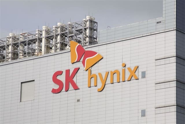
SK Hynix is examining Miyagi Prefecture in northeastern Japan as a potential location for a large-scale memory semiconductor manufacturing facility, according to the company. The South Korean memory giant stressed that internal discussions remain at an exploratory stage and no investment decision has been finalized.
The move reflects a broader pattern of Asian semiconductor manufacturers seeking capacity outside their home markets, driven by supply chain diversification and government incentives. Miyagi, approximately 300 kilometers north of Tokyo, has emerged as a candidate site as SK Hynix evaluates infrastructure, workforce availability, and regional support packages.
Japan's Semiconductor Courtship
Tokyo has committed tens of billions of dollars to revive domestic chip production through direct subsidies and tax incentives. The government's strategy centers on attracting foreign chipmakers to build advanced manufacturing capacity on Japanese soil, particularly in memory and logic segments where the country ceded leadership over the past two decades.
SK Hynix's consideration of a Japanese fab follows similar commitments by Taiwan Semiconductor Manufacturing Company, which is constructing a facility in Kumamoto Prefecture with Sony and Denso as local partners. Micron Technology announced plans in 2023 to invest up to 500 billion yen in its Hiroshima production lines over the next decade, backed by Japanese subsidies.
For SK Hynix, a Japan facility would mark a significant geographic expansion beyond its existing manufacturing footprint in South Korea, China, and the United States. The company operates DRAM and NAND flash production in Icheon and Cheongju, with additional capacity in Wuxi, China, subject to ongoing export control scrutiny.
Infrastructure and Workforce Calculus
Miyagi offers several advantages as a potential fab location. The prefecture maintains industrial infrastructure developed through decades of electronics and automotive manufacturing. Tohoku University, based in Miyagi's capital city of Sendai, produces engineering graduates in materials science and electrical engineering, providing a local talent pipeline.
However, the region also faces demographic headwinds common across Japan. Miyagi's population has declined roughly 4 percent since 2010, and the prefecture competes with Tokyo and other metropolitan areas for skilled workers. Any major semiconductor investment would likely require recruiting engineers from across Japan and potentially overseas.
Local governments in Japan typically assemble support packages that include land acquisition assistance, infrastructure improvements, and workforce training programs. Miyagi officials have not publicly disclosed the terms of any proposal presented to SK Hynix, and the company declined to comment on specific incentives under consideration.
Timing and Capacity Questions
SK Hynix has not indicated the scale of investment, production capacity, or timeline for a potential Miyagi facility. Industry observers note that greenfield memory fabs typically require three to five years from groundbreaking to volume production, with capital expenditures ranging from 5 billion to 20 billion dollars depending on technology node and monthly wafer output.
The company's cautious framing suggests internal debate over the strategic and financial merits. Memory markets remain cyclical, and SK Hynix reported operating losses in 2023 before returning to profitability in 2024 as demand recovered. Management has emphasized discipline in capacity additions, particularly as the industry navigates uncertainty around artificial intelligence server demand and consumer electronics refresh cycles.
A Japan facility could serve multiple strategic purposes. It would diversify manufacturing risk away from South Korea and China, provide closer proximity to Japanese customers in automotive and industrial segments, and potentially qualify SK Hynix for government subsidies that improve project economics.
Regional Chip Ambitions
Japan's semiconductor revitalization effort extends beyond attracting foreign manufacturers. The government has backed Rapidus, a domestic consortium aiming to produce two-nanometer logic chips by 2027 with IBM technology, though the venture faces skepticism over its aggressive timeline and reliance on unproven manufacturing processes.
SK Hynix's exploration of a Japanese investment comes as memory demand shows signs of stabilization after a sharp downturn. High-bandwidth memory used in AI accelerators has driven margin expansion, while traditional DRAM and NAND markets remain oversupplied. The company's capital allocation decisions will hinge on demand visibility and the relative returns available across potential projects.
For now, Miyagi remains one option among several as SK Hynix weighs its next manufacturing expansion. The company's emphasis that no decision has been made reflects the complexity of multibillion-dollar fab commitments in an industry where timing and location can determine profitability for decades.
RELATED STORIES
Tokyo Summit Pushes Trilateral Tech Alliance Among Taiwan, Japan, and US
Cheng Wei-Lun · 3 min
Korean Coffee Chain Paik's Opens First Tokyo Locations
Cheng Wei-Lun · 3 min
Japanese Automakers Turn to Startups for Self-Driving Technology
Aiko Nakamura · 2 min
Japan Launches First Oncolytic Virus Therapy for Esophageal Cancer
Aiko Nakamura · 3 min
Spot something wrong? Email editor@briefasia.com. We log every correction publicly.