Technology · Dev
Samsung Unveils zHBM and V10 BV-NAND to Address AI Memory Bottleneck
New 3D memory architectures and processor-memory integration aim to ease data movement constraints as AI workloads scale
KEY TAKEAWAYS
- ·Samsung Electronics announced zHBM and V10 BV-NAND architectures targeting AI memory bottlenecks through tighter processor-memory integration and vertical NAND scaling.
- ·The new designs address data movement constraints and power consumption as AI workloads strain existing memory systems in data center deployments.
- ·Competition intensifies across Asia's memory sector as SK Hynix gains HBM market share and Chinese manufacturers ramp DDR5 production for AI infrastructure.
New Memory Architectures Target AI Scaling Challenges
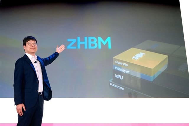
Samsung Electronics is rolling out two new memory concepts designed to address the bottleneck forming between processors and memory as artificial intelligence workloads expand. The company announced zHBM and V10 BV-NAND architectures that prioritize tighter processor-memory integration and three-dimensional design improvements, according to Samsung.
The moves come as AI training and inference operations increasingly strain existing memory systems. Current architectures struggle to move data fast enough between compute units and storage, creating performance ceilings that limit how effectively AI models can scale. Power consumption during data transfer has also emerged as a critical constraint in data center deployments.
zHBM Brings Processor-Memory Closer
Samsung's zHBM concept centers on reducing the physical distance between high-bandwidth memory and processing units. Traditional HBM stacks sit adjacent to GPUs or AI accelerators, but zHBM explores vertical integration that shortens data paths and cuts latency.
The approach addresses what engineers call the "memory wall," where processors sit idle waiting for data to arrive from memory modules. By shrinking the path between compute and storage, Samsung aims to keep AI accelerators fed with data more consistently, lifting utilization rates and reducing wasted cycles.
Tighter integration also promises power savings. Data movement consumes significant energy in AI systems, sometimes rivaling the compute operations themselves. Shorter interconnects require less voltage to drive signals, trimming power budgets at the rack level.
V10 BV-NAND Pushes 3D Density Higher
The V10 BV-NAND architecture represents Samsung's latest push in vertical NAND scaling. BV-NAND, or bonded vertical NAND, stacks memory cells in three dimensions using wafer-bonding techniques that bypass some of the physical limits facing single-wafer designs.
Samsung's V10 generation targets higher cell densities and improved read-write performance for AI training datasets and model checkpoints. As AI models grow past a trillion parameters, storage capacity and throughput become bottlenecks just as critical as compute power.
The architecture also addresses endurance concerns. AI training workloads write massive volumes of intermediate data, wearing out NAND cells faster than consumer applications. V10 BV-NAND incorporates error correction and wear-leveling mechanisms tuned for data center write patterns.
Asia's Memory Race Intensifies
Samsung's announcements arrive amid fierce competition across Asia's memory sector. SK Hynix has gained ground in the HBM market, securing major design wins with Nvidia and other AI chip makers. CXMT in China continues to ramp DDR5 production, while Japanese manufacturers explore specialty memory for edge AI applications.
The regional dynamics reflect broader supply chain realignments. AI infrastructure spending is concentrating in hyperscalers and cloud providers, most of whom operate significant capacity in Singapore, Tokyo, and Seoul. Memory makers are positioning products not just for performance, but for the thermal and power envelopes these facilities demand.
Samsung's focus on data movement efficiency aligns with a shift in AI system design. Early AI accelerators prioritized raw compute throughput, measured in teraflops or petaflops. Now, architects increasingly optimize for memory bandwidth and energy efficiency, recognizing that data transfer often determines real-world performance.
Manufacturing and Deployment Timeline
Samsung has not disclosed volume production timelines for zHBM or V10 BV-NAND. Both remain in the concept or early development phase, with commercial availability likely several quarters out. The company typically moves from architecture announcements to qualification samples within 12 to 18 months, followed by mass production ramp.
Industry observers expect initial deployments in high-margin AI training clusters, where customers tolerate premium pricing for performance gains. Broader adoption in inference workloads and edge devices would follow as yields improve and costs decline.
The memory wall challenge is unlikely to ease soon. AI models continue growing in size and complexity, while training datasets expand into multi-petabyte ranges. Memory bandwidth and capacity will remain critical constraints, ensuring sustained demand for architectural innovation across the semiconductor sector.
RELATED STORIES
Samsung Closes Yield Gap in Memory Race with SK Hynix
Cheng Wei-Lun · 3 min
SK Hynix Reviews Future of China Packaging Facility Amid $3 Billion Valuation Talk
Cheng Wei-Lun · 2 min

Samsung Doubles BOE Panel Orders as Chinese Suppliers Tighten Grip on TV Display Market
Cheng Wei-Lun · 3 min

Seoul Warns Against Redistributing Chip Profits as China Investment Accelerates
Jun-ho Seo · 2 min
Spot something wrong? Email editor@briefasia.com. We log every correction publicly.