Technology · Dev
Samsung Unveils Vertical Memory Stack and 400-Layer NAND at FMS Conference
Korean chipmaker shows prototypes of stacked-on-logic HBM and bonded NAND architecture targeting AI infrastructure demands
KEY TAKEAWAYS
- ·Samsung Electronics revealed zHBM stacked-on-logic and zNAND-O concepts alongside a 400-plus-layer NAND chip built with wafer bonding at the Future of Memory and Storage conference.
- ·The 400-layer NAND uses wafer bonding to exceed traditional deposition limits, targeting lower cost per terabyte for hyperscale data centers and enterprise storage.
- ·Samsung faces intensifying competition from SK hynix in HBM shipments to Nvidia and from YMTC in high-layer NAND, making roadmap execution critical to market share.
Samsung Pushes 3D Memory Frontiers
Samsung Electronics showed off three new memory architectures at the Future of Memory and Storage conference, presenting concepts that stack high-bandwidth memory directly onto logic chips and a NAND flash design exceeding 400 layers, according to Samsung.
The Korean chipmaker unveiled two experimental models: zHBM, which places high-bandwidth memory vertically above processing logic, and zNAND-O, a vertically oriented NAND configuration. Both designs represent a shift toward three-dimensional integration as the industry races to meet the bandwidth and density requirements of AI training clusters and inference workloads.
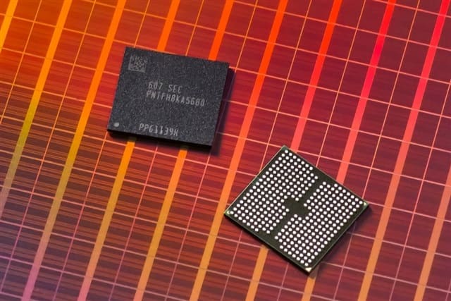
Samsung disclosed the 400-layer NAND for the first time at the conference. The chip relies on wafer bonding, a technique that fuses separately fabricated silicon wafers to achieve layer counts that would be impractical using conventional deposition methods. The move places Samsung in direct competition with Micron and SK hynix, both of which have announced or sampled ultra-high-layer NAND products over the past year.
Stacking Memory on Logic
The zHBM concept stacks high-bandwidth memory dies directly atop logic circuits, reducing the physical distance data must travel between compute and memory. This vertical arrangement can cut latency and power consumption, two persistent bottlenecks in AI accelerators and graphics processors.
Current HBM packages sit beside or beneath GPU dies, connected through silicon interposers or organic substrates. By placing memory on top of logic, Samsung aims to shorten interconnect paths and free up package real estate for additional compute or I/O components.
The company has not disclosed a production timeline for zHBM, and technical challenges remain. Thermal management becomes more complex when memory and logic share a vertical stack, and manufacturing yield depends on aligning and bonding multiple dies with sub-micron precision.
Bonded NAND Reaches 400 Layers
Samsung's 400-layer NAND relies on wafer bonding to combine separately built memory structures. Traditional 3D NAND grows layers sequentially, but process complexity and aspect-ratio limits make it difficult to exceed 300 layers in a single stack. Bonding allows manufacturers to build two or more shorter stacks and fuse them, effectively doubling or tripling achievable layer counts.
The technique has gained traction as NAND suppliers push density to reduce cost per terabyte. Higher layer counts mean more storage capacity per wafer, which translates to lower production costs for hyperscale data centers purchasing petabyte-scale arrays.
Samsung has not specified when the 400-layer NAND will enter mass production or which product lines will adopt the technology first. Enterprise SSDs and data-center arrays are likely initial targets, given their tolerance for higher unit costs during early production ramps.
Asia's Memory Race Intensifies
The announcements position Samsung to defend its share in both NAND and DRAM markets, where competition from SK hynix and Chinese suppliers has intensified. SK hynix currently leads in HBM shipments to Nvidia, while Micron has ramped its own high-bandwidth memory production. Samsung's HBM3E products have faced qualification delays at some AI accelerator customers, adding urgency to its roadmap execution.
In NAND, Samsung competes with Kioxia and Western Digital in Japan, SK hynix in Korea, and YMTC in China. YMTC has demonstrated 232-layer NAND and is believed to be developing bonded architectures, though U.S. export controls limit its access to advanced lithography and process equipment.
Samsung's decision to preview experimental concepts at FMS signals confidence in its development pipeline, but also reflects the need to reassure customers and investors that it remains on pace with rivals. The memory market has cycled through oversupply and tight capacity over the past two years, and AI-driven demand has shifted purchasing power toward hyperscalers and cloud providers who favor suppliers with clear technology roadmaps.
The zHBM and zNAND-O concepts remain in early stages, and production-ready versions may differ substantially from the prototypes shown at FMS. Still, the 400-layer NAND disclosure suggests Samsung has moved beyond internal development and is preparing qualification samples for key customers. How quickly those designs reach volume production will determine whether Samsung can reclaim momentum in the memory sector.
RELATED STORIES

South Korea Records Highest September Export Start on Semiconductor Demand
Tran Quoc Bao · 3 min

Memory Makers Gain Leverage as AI Server Costs Climb
Cheng Wei-Lun · 3 min

Samsung and SK Hynix Turn Down KEPCO's Multibillion-Dollar Prepayment Demand
Cheng Wei-Lun · 4 min

Samsung's Device Division Reports First Quarterly Loss as Chip Costs Surge
Cheng Wei-Lun · 3 min
Spot something wrong? Email editor@briefasia.com. We log every correction publicly.