Technology · Dev
Samsung Plans 50-Unit Hybrid Bonding Line at Pyeongtaek for Advanced Memory
South Korean chipmaker expands die-to-wafer bonding capacity for HBM and logic production as equipment negotiations continue
KEY TAKEAWAYS
- ·Samsung is preparing a die-to-wafer hybrid bonding line with approximately 50 bonders at its Pyeongtaek campus for next-generation HBM and logic production.
- ·Extended pricing negotiations have led Samsung to evaluate multiple equipment suppliers, including South Korean manufacturers seeking to capture share in the hybrid bonding market.
- ·The facility will support HBM4 mass production and foundry chiplet designs, positioning Samsung to compete with TSMC and Intel in advanced packaging capacity.
Scaling Advanced Packaging in South Korea
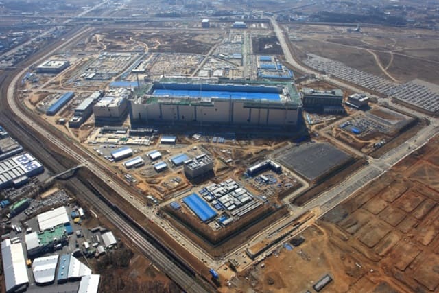
Samsung Electronics is constructing a die-to-wafer hybrid bonding production line at its Pyeongtaek campus, planning to deploy roughly 50 bonding tools for next-generation high-bandwidth memory and logic chip manufacturing. The line will support the company's push into advanced packaging technologies critical for AI accelerators and data-center applications.
The scale of the installation reflects Samsung's ambition in hybrid bonding, a technique that stacks chip dies with sub-micron alignment and direct copper-to-copper connections. Unlike traditional microbump approaches, hybrid bonding eliminates the need for solder and enables tighter pitch, higher bandwidth, and lower power consumption. These attributes matter especially for HBM4, the next iteration of memory stacks powering training clusters at hyperscalers.
Equipment Sourcing and Regional Dynamics
Samsung is evaluating multiple suppliers for the bonding equipment, including South Korean manufacturers alongside established vendors. Pricing negotiations have extended longer than initially expected, prompting the company to widen its supplier search within the domestic ecosystem. Korean equipment makers have been investing heavily in hybrid bonding technology, seeking to capture share in a market historically dominated by European and Japanese firms.
The decision on supplier mix will influence not only capital expenditure but also ramp timelines and yield learning curves. Hybrid bonding remains a relatively immature process, and tool performance can vary significantly across vendors. Samsung's Pyeongtaek campus already houses multiple memory fabrication lines and advanced packaging facilities, offering logistical advantages for integrating the new bonding capacity.
HBM and Logic Integration
High-bandwidth memory has become a strategic priority for Samsung as it competes with SK hynix in supplying Nvidia, AMD, and other AI chip designers. HBM4, expected to enter mass production in late 2026 or early 2027, will likely incorporate hybrid bonding between the logic base die and the first DRAM die in the stack. This architectural shift promises to boost data rates beyond 1.5 terabytes per second per stack while reducing thermal bottlenecks.
Beyond memory, Samsung's foundry business is exploring hybrid bonding for advanced logic packaging, particularly for chiplet-based designs. Clients designing multi-die processors for AI inference and edge computing stand to benefit from the tighter interconnect density. The Pyeongtaek line is expected to serve both memory and foundry customers, though initial volumes will likely prioritize HBM production given current market demand.
Regional Capacity Race
Samsung's move comes as Taiwan's TSMC and Intel both accelerate their own hybrid bonding roadmaps. TSMC's SoIC technology has been in limited production since 2023, and the company is expanding capacity at its竹南 advanced packaging site. Intel's Foveros Direct, another hybrid bonding variant, is slated for volume production in its New Mexico and Arizona facilities. The parallel buildouts underscore the industry's consensus that hybrid bonding will be essential for maintaining Moore's Law economics as monolithic scaling slows.
South Korea's semiconductor equipment sector stands to gain if Samsung's procurement tilts toward domestic suppliers. The government in Seoul has committed tens of billions of dollars in subsidies and tax incentives to bolster the local chip ecosystem, viewing equipment self-sufficiency as a strategic imperative. However, Samsung's final vendor selection will hinge on technical performance and cost, not solely on national preference.
The 50-bonder line represents one of the largest single hybrid bonding investments announced to date in Asia. Assuming each tool can process several hundred wafers per week at maturity, the facility could support annual production in the range of hundreds of thousands of bonded wafers, enough to supply multiple HBM4 programs and early foundry engagements. Samsung has not disclosed a target start date for volume production, but industry timelines suggest equipment installation could begin in the second half of 2026.
RELATED STORIES

South Korea Taps Three Telecom Giants to Deliver Free AI Services Nationwide
Cheng Wei-Lun · 3 min
Memory Makers Gain Leverage as AI Server Costs Climb
Cheng Wei-Lun · 3 min
Samsung Display Restarts Asan OLED Campus as Foldable Phones Stage Recovery
Cheng Wei-Lun · 4 min
Samsung's Device Division Reports First Quarterly Loss as Chip Costs Surge
Cheng Wei-Lun · 3 min
Spot something wrong? Email editor@briefasia.com. We log every correction publicly.