Technology · Dev
Musk Unveils $16.8 Billion Terafab Investment With FEL Light Source Hint
The Tesla and SpaceX founder signals a push into chip manufacturing infrastructure with a massive initial commitment and advanced lithography ambitions.
KEY TAKEAWAYS
- ·Elon Musk announced a $16.8 billion initial investment in Terafab, a large-scale wafer fabrication facility, with concept images suggesting free-electron laser technology plans.
- ·Free-electron lasers could enable sub-2-nanometer chip production, but no commercial FEL lithography tool exists today and technical challenges around size and power remain significant.
- ·The project positions Musk in the global semiconductor manufacturing race alongside TSMC and Intel, though Terafab has not disclosed target nodes, timeline, or whether it will seek U.S. CHIPS Act subsidies.
A New Frontier for Musk
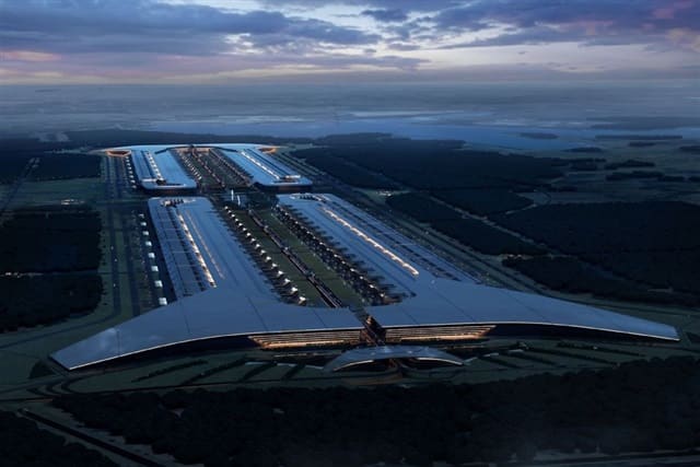
Elon Musk has expanded his industrial footprint once again, this time targeting semiconductor manufacturing. The entrepreneur disclosed a $16.8 billion initial investment in Terafab, a large-scale wafer fabrication facility, according to Musk's announcement. Alongside the funding figure, he presented concept images of the completed facility that include visual references to free-electron laser (FEL) light source technology.
The move positions Musk alongside a small cohort of industrialists willing to commit tens of billions to advanced chip production infrastructure. Terafab's scale and the technology hinted at in the concept renders suggest ambitions that extend beyond conventional extreme ultraviolet (EUV) lithography.
FEL and the Next Lithography Race
Free-electron lasers represent a potential successor to current EUV systems, which rely on laser-produced plasma to generate 13.5-nanometer wavelength light. FEL systems can produce even shorter wavelengths with higher brightness and stability, opening a path to sub-2-nanometer node manufacturing without the complexity of high-numerical-aperture optics.
ASML, the Dutch lithography giant and sole supplier of EUV scanners, has publicly explored FEL-EUV as a long-term roadmap option. The company has invested in research partnerships with synchrotron and accelerator facilities across Europe and the United States to evaluate FEL feasibility for volume production. However, no commercial FEL lithography tool exists today, and the technical challenges remain formidable. FEL systems require particle accelerators hundreds of meters long, raising questions about fab footprint, power consumption, and integration with existing process flows.
Musk's concept imagery does not confirm a commitment to FEL, but the inclusion of the technology in promotional materials signals interest. If Terafab pursues FEL lithography, it would be the first private fab to attempt commercialization of the approach. That would also create a dependency on ASML or a yet-to-emerge competitor to deliver the tooling, or alternatively, force Musk to develop proprietary lithography systems in-house.
Capital and Context
The $16.8 billion figure disclosed by Musk represents the initial phase of investment. Modern leading-edge fabs often require $20 billion to $30 billion in total capital expenditure before reaching full production capacity. TSMC's Arizona facilities, for example, carry a projected cost exceeding $40 billion across multiple phases.
Terafab's funding announcement arrives amid a broader wave of semiconductor manufacturing investment across the United States, Europe, and Asia. The U.S. CHIPS and Science Act has allocated $52 billion in subsidies and tax credits to encourage domestic production, while the European Chips Act targets €43 billion in public and private investment. Japan and South Korea have each committed multi-billion-dollar packages to retain and expand fab capacity.
Musk has not specified whether Terafab will apply for CHIPS Act funding, nor has he detailed the facility's target nodes, production timeline, or customer base. The project's success will depend on securing equipment suppliers, process technology partners, and anchor customers willing to commit wafer volume years in advance.
Strategic Implications
Musk's entry into wafer manufacturing adds a new variable to the global semiconductor supply chain. Tesla has long been a significant consumer of automotive-grade chips, and the company has developed custom silicon for its Full Self-Driving computer and Dojo training platform. Vertical integration into fab operations would give Tesla control over supply, cost, and roadmap timing, a strategic advantage in a capital-intensive industry with long lead times.
However, operating a leading-edge fab requires expertise in process integration, yield management, and equipment maintenance that Musk's existing ventures do not possess. Partnerships with established foundries or equipment makers will likely be necessary. ASML's interest in FEL-EUV could align with Terafab's needs, but any collaboration would require years of joint development before production readiness.
The concept images released by Musk offer limited technical detail, and no construction timeline has been announced. Industry observers will watch for site selection, permitting filings, and equipment orders as indicators of project momentum. Until then, Terafab remains a high-capital bet on a technology transition that has yet to prove itself at scale.
RELATED STORIES
Lenovo Accelerates Toward $100 Billion Revenue on AI Momentum
Cheng Wei-Lun · 3 min

Pangilinan Eyes Tarlac Tech Hub With Power, Data Centers and Connectivity
Mariel D. Santos · 4 min

South Korea Commits $880 Billion to AI and Chip Infrastructure
Jun-ho Seo · 3 min
Formosa Plastics and Daicel Launch Chip Materials Joint Venture in Taiwan
Cheng Wei-Lun · 3 min
Spot something wrong? Email editor@briefasia.com. We log every correction publicly.