Technology · AI
Memory Shortage Eclipses Chip Manufacturing as AI Industry Bottleneck
Advanced packaging capacity and memory allocation emerge as the new constraints in the semiconductor race, outpacing even foundry availability
KEY TAKEAWAYS
- ·Memory chip availability and advanced packaging capacity have replaced foundry access as the primary constraint limiting AI hardware production, with HBM lead times extending beyond twelve months.
- ·TSMC, ASE, and Amkor packaging facilities report utilization above 95 percent, forcing customers to negotiate integrated supply agreements spanning wafer fabrication, memory, and assembly.
- ·Asian governments including South Korea, Japan, and Malaysia are investing billions in domestic packaging infrastructure to reduce dependence on Taiwan-based providers through 2030.
The New Constraint
The semiconductor industry has reached an inflection point where memory availability, not chip manufacturing capacity, defines the pace of AI infrastructure buildout. Leading foundries report their advanced nodes fully allocated through the coming quarters, yet the more acute pressure now sits with memory suppliers and packaging facilities struggling to keep pace with demand from hyperscalers and AI system builders.
This represents a structural shift in where bottlenecks appear across the supply chain. For two years, the race centered on securing wafer capacity at TSMC's Arizona and Taiwan fabs, Samsung's Pyeongtaek lines, and Intel's Ohio operations. Today, those slots remain scarce, but the binding constraint has moved downstream to high-bandwidth memory production and the specialized packaging required to marry logic and memory into functioning AI accelerators.
Industry observers note that HBM production lines at SK hynix, Samsung, and Micron are sold out well into 2027, with lead times stretching beyond twelve months for some specifications. The mismatch between logic chip output and available memory creates a coordination problem: even companies holding foundry allocations find themselves unable to ship complete systems without corresponding memory supply.
Packaging Emerges as Critical Path
Advanced packaging facilities, particularly those capable of chiplet integration and 2.5D stacking, face similar strain. TSMC's CoWoS capacity, ASE's fan-out lines, and Amkor's advanced assembly operations all report utilization above 95 percent, with customers competing for slots through a combination of volume commitments and long-term agreements.
The packaging bottleneck affects not only established players but also the wave of AI chip startups seeking to bring custom silicon to market. Securing a few thousand wafers at a foundry no longer guarantees a path to production if packaging capacity cannot be locked in parallel. This dynamic favors larger customers with the scale to negotiate integrated supply agreements spanning wafer fabrication, memory procurement, and final assembly.
Several Asian governments have responded by announcing support for domestic packaging infrastructure. South Korea's semiconductor strategy includes USD 4.7 billion earmarked for advanced packaging through 2030, while Malaysia and Vietnam position themselves as alternative hubs for assembly and test operations. Japan's LSTC consortium, backed by Tokyo and involving Toyota, Sony, and NTT, aims to build domestic capacity for chiplet integration to reduce reliance on Taiwan-based providers.
Memory Architecture Divergence
The memory shortage has accelerated architectural experimentation. Some hyperscalers explore alternatives to HBM, including GDDR6X in cost-sensitive inference workloads and novel memory-near-compute designs that reduce bandwidth requirements by moving processing closer to storage. Others double down on securing HBM3E supply, accepting higher costs and longer lead times to maintain performance leadership in training clusters.
This bifurcation mirrors a broader trend in AI chip design: the market is splitting between high-performance training accelerators, where memory bandwidth remains paramount, and inference chips optimized for throughput and efficiency, where architectural trade-offs can mitigate memory constraints. The former demands cutting-edge packaging and the latest HBM generations; the latter opens design space for alternative approaches.
Chinese AI chip developers face compounded challenges. Export controls restrict access to both leading-edge logic nodes and advanced packaging services, while memory suppliers navigate compliance requirements that limit HBM shipments to certain customers. This has driven investment in domestic packaging capabilities and alternative memory solutions, though the technology gap remains significant.
Supply Chain Realignment
The current environment rewards companies that secured multi-year supply agreements early. NVIDIA's partnerships with SK hynix and TSMC, covering both memory and packaging, illustrate the strategic advantage of vertical coordination. Startups and smaller players, by contrast, must navigate spot markets with volatile pricing and limited availability, or accept constraints that delay product launches.
Foundries and packaging providers have begun requiring customers to commit to memory procurement as part of integrated contracts, effectively bundling supply across the stack. This shifts negotiating power further toward suppliers and raises barriers for new entrants lacking the volume or relationships to secure comprehensive agreements.
The memory and packaging crunch also influences geographic diversification strategies. While companies seek to de-risk supply chains by spreading production across regions, the concentration of advanced packaging in Taiwan and HBM production in South Korea limits options. Efforts to build alternative capacity in the United States, Europe, and Southeast Asia will take years to reach meaningful scale, leaving the current bottlenecks in place through at least 2028.
The Path Forward
Industry roadmaps point toward incremental relief. Memory suppliers plan capacity expansions targeting 2027 and 2028 ramp dates, while packaging providers invest in next-generation lines. Whether these additions suffice depends on the trajectory of AI demand, which continues to surprise on the upside as new applications and model architectures drive hardware consumption.
In the near term, the semiconductor ecosystem must navigate a period where memory and packaging define the pace of growth, not transistor scaling or foundry output. This reality reshapes competitive dynamics, favoring scale, long-term planning, and supply chain integration over pure design innovation. The companies that adapt quickest to this new constraint will capture disproportionate value as the AI infrastructure buildout continues.
RELATED STORIES
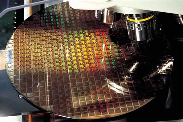
TSMC Shifts CoW Packaging Work to Third-Party Contractors as AI Demand Strains Capacity
Cheng Wei-Lun · 3 min

Samsung Electro-Mechanics Widens Materials Tie-Up for Glass Substrate AI Chips
Cheng Wei-Lun · 2 min
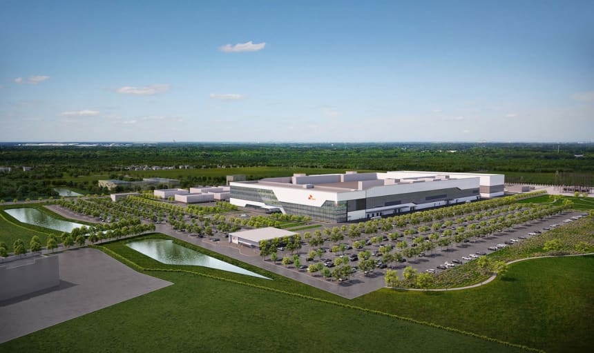
SK Hynix Breaks Ground on $3.9 Billion Chip Packaging Facility in Indiana
Cheng Wei-Lun · 3 min
Intel's Gelsinger Dismisses HBM as 'Lousy' While SK Hynix Signals Search for Successor
Cheng Wei-Lun · 3 min
Spot something wrong? Email editor@briefasia.com. We log every correction publicly.