Technology · Dev
Intel's Gelsinger Dismisses HBM as 'Lousy' While SK Hynix Signals Search for Successor
The AI memory architecture that powers today's chips faces growing skepticism from industry leaders who see fundamental limitations ahead
KEY TAKEAWAYS
- ·Former Intel CEO Pat Gelsinger called high-bandwidth memory 'lousy' at a Paris AI summit while SK Hynix acknowledged the technology is not the final solution to AI memory constraints.
- ·SK Hynix commands the largest share of the HBM market but publicly stated the architecture has fundamental limits as AI model demands outpace memory bandwidth improvements.
- ·The industry is exploring compute-in-memory, optical interconnects, and new materials as successors, with Asia's memory leaders racing to control the next-generation architecture.
A Blunt Assessment at the Paris Summit
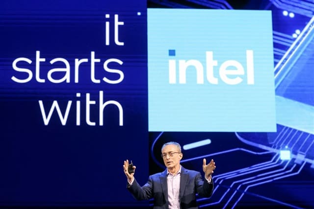
Former Intel CEO Pat Gelsinger used unusually blunt language to describe high-bandwidth memory at an AI summit in Paris, calling the technology "lousy." The comment came as industry attention intensifies on the memory architecture that has become central to AI chip design, particularly for training and inference workloads.
HBM has emerged as the dominant memory solution for AI accelerators over the past three years, stacking multiple DRAM dies vertically to achieve bandwidth levels conventional memory cannot match. Nvidia's H100 and H200 chips, AMD's MI300 series, and Google's TPUs all rely on the technology. Yet Gelsinger's critique reflects growing recognition that HBM may represent an interim step rather than a lasting solution.
SK Hynix Acknowledges the Limits
SK Hynix, which commands the largest share of the HBM market, has stated publicly that the technology is not the final answer to AI memory bottlenecks. The South Korean manufacturer's acknowledgment carries weight given its position: the company supplies HBM3 and HBM3E to Nvidia and has invested billions in production capacity.
The admission signals that even those profiting most from HBM see architectural constraints ahead. Current HBM generations deliver bandwidth exceeding 819 gigabytes per second, but AI models continue to grow in parameter count and context length at rates that outpace memory improvements. Training runs for frontier models already consume thousands of accelerators, with memory bandwidth often the limiting factor in scaling efficiency.
The Search for What Comes Next
Industry engineers point to several fundamental challenges with HBM. The technology requires complex through-silicon vias and microbump connections, driving up manufacturing costs and limiting yield rates. Thermal management becomes more difficult as die counts increase. Power consumption remains high relative to the data transferred. Most critically, the physical constraints of vertical stacking impose hard limits on how much further bandwidth can scale.
Multiple research directions have emerged as potential successors. Compute-in-memory architectures move processing closer to where data sits, reducing the need to shuttle information across buses. Optical interconnects promise orders-of-magnitude bandwidth improvements by replacing electrical signaling with photonics. New materials like phase-change memory and resistive RAM offer different trade-offs in speed, density, and power.
Samsung and Micron, SK Hynix's primary competitors, are also exploring alternatives. Samsung has demonstrated prototype chips integrating HBM with processing-in-memory capabilities. Micron has invested in near-memory computing approaches that distribute logic across the memory array itself.
Asia's Memory Race Intensifies
The push beyond HBM carries strategic implications for Asia's semiconductor industry. South Korea, through SK Hynix and Samsung, controls roughly 95 percent of the HBM market. Japan's Kioxia and Taiwan's Nanya have announced plans to enter production but trail by at least two generations. China's CXMT faces export controls that limit access to the advanced packaging equipment HBM requires.
Whoever develops the successor technology will capture not just market share but also influence over AI infrastructure architecture for the next decade. Governments across the region have increased subsidies for memory R&D accordingly. South Korea's semiconductor support package, announced earlier this year, dedicates significant funding to next-generation memory. Japan's Rapidus initiative includes memory integration as a core objective.
What the Critique Reveals
Gelsinger's dismissal of HBM as "lousy" reflects a broader industry debate about whether incremental improvements to existing memory hierarchies can keep pace with AI's demands. Intel itself has pursued alternative approaches, including integrating high-bandwidth cache directly on package with its Ponte Vecchio architecture and exploring magnetic RAM for certain workloads.
The critique also underscores tension between hardware realities and AI ambitions. Model developers want unlimited context windows and real-time inference on multi-modal inputs. Memory engineers face physics: electrons can only move so fast through silicon, and stacking more dies eventually creates more problems than it solves.
SK Hynix's concurrent acknowledgment that HBM is not the final answer suggests the industry has reached a consensus: the current approach buys time but does not solve the underlying mismatch between compute capability and memory bandwidth. The race now centers on which architecture will emerge to replace it, and which companies will control that transition.
RELATED STORIES
Samsung Eyes Vietnam for Legacy Memory Backend as HBM Demand Tightens Capacity
Cheng Wei-Lun · 3 min
Samsung Closes Gap on SK Hynix With Sharp HBM4 Yield Gains
Cheng Wei-Lun · 2 min

South Korea Commits $880 Billion to AI and Chip Infrastructure
Jun-ho Seo · 3 min

US Expert Warns Seoul's Tech Regulation May Strain Bilateral Alliance
Cheng Wei-Lun · 3 min
Spot something wrong? Email editor@briefasia.com. We log every correction publicly.