Technology · Dev
Inversion Semiconductor Builds Particle-Accelerator Lithography to Challenge ASML's EUV Dominance
The startup claims its X-ray platform can achieve shorter wavelengths and higher throughput than current extreme ultraviolet systems, opening a new path to sub-2nm chip manufacturing.
KEY TAKEAWAYS
- ·Inversion Semiconductor is building a particle-accelerator lithography platform designed to exceed ASML's EUV systems in wavelength, throughput, and chip density.
- ·The X-ray approach targets sub-2nm chip production, where current EUV tools face resolution limits and require costly multi-patterning techniques.
- ·Commercialization faces decade-long timelines and billions in capital, with foundry partnerships and production-scale validation still unproven.
A New Contender in Advanced Lithography
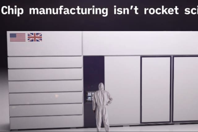
Inversion Semiconductor has unveiled plans for a particle-accelerator-based lithography platform designed to surpass the capabilities of existing extreme ultraviolet systems in wavelength, throughput, and chip density. The company positions its X-ray approach as an alternative pathway for chipmakers seeking to push beyond the physical limits of current EUV technology.
The announcement arrives as semiconductor manufacturers face mounting pressure to deliver sub-2nm process nodes while managing the escalating cost and complexity of lithography equipment. ASML currently holds a monopoly on high-NA EUV systems, with each machine priced above $350 million and requiring extensive infrastructure support.
Technical Architecture and Claims
Inversion Semiconductor's platform relies on particle acceleration to generate X-rays with wavelengths shorter than the 13.5nm light produced by contemporary EUV tools. Shorter wavelengths enable finer pattern resolution, a critical requirement for packing more transistors onto silicon as Moore's Law approaches its theoretical boundaries.
The company asserts that its system will deliver higher wafer throughput than current-generation EUV scanners, which typically process 160 to 220 wafers per hour depending on pattern complexity and layer count. Throughput remains a bottleneck in advanced node production, where a single chip may require dozens of EUV exposure steps.
By combining shorter wavelengths with improved throughput, Inversion aims to enable denser chip architectures without the multi-patterning techniques that add cost and cycle time to leading-edge fabrication. Multi-patterning currently accounts for a significant portion of process complexity at the 3nm and 2nm nodes, where features approach the resolution limit of 13.5nm EUV light.
Asia's Lithography Landscape
The development carries strategic weight across Asia's semiconductor ecosystem. Taiwan Semiconductor Manufacturing Company, Samsung Foundry, and Intel all operate advanced fabs in the region and are racing to deploy sub-2nm processes by 2027. Each has invested heavily in ASML's EUV roadmap, but diversification of lithography suppliers would reduce concentration risk and potentially accelerate innovation cycles.
Japan and South Korea have prioritized domestic lithography capabilities in recent industrial policy, though neither has produced a commercial alternative to ASML's EUV systems. China's efforts to develop indigenous lithography tools have focused on deep ultraviolet technology, leaving a gap in EUV and next-generation platforms.
Inversion's particle-accelerator approach represents a different technical bet than incremental improvements to reflective optics or light-source power, the two main vectors of EUV advancement pursued by ASML and its suppliers. If proven viable at production scale, the architecture could reshape capital allocation decisions across the foundry sector.
Commercialization Hurdles
Translating laboratory demonstrations into production-worthy lithography tools has historically required a decade or more of engineering and billions in capital. ASML spent over fifteen years and approximately $6 billion developing EUV from initial prototypes to the first commercial shipments in 2018. The company benefited from sustained R&D partnerships with TSMC, Samsung, and Intel, which provided both funding and real-world process feedback.
Inversion Semiconductor has not disclosed the current maturity of its platform, the timeline to alpha tools, or the identity of foundry partners willing to co-develop the technology. Lithography startups face challenges securing the iterative design cycles and fab access necessary to prove reliability, overlay accuracy, and defect performance at the levels demanded by leading-edge production.
Particle-accelerator systems also introduce unique engineering constraints. Generating and controlling high-energy particle beams at the precision required for nanometer-scale patterning demands advances in beam optics, thermal management, and vibration isolation. The physical footprint and power consumption of accelerator-based tools may exceed those of conventional EUV scanners, affecting fab layout and operating economics.
Market Implications
The semiconductor capital equipment market has consolidated around a small number of suppliers for critical process steps, with ASML holding an effective monopoly in EUV lithography. Any credible alternative platform would attract attention from chipmakers seeking leverage in equipment negotiations and insurance against supply disruptions.
Foundries operating at the technology frontier typically maintain multi-year equipment roadmaps locked to specific lithography architectures. Introducing a new platform mid-cycle would require significant process re-qualification and mask infrastructure changes, creating switching costs that favor incumbents. Early engagement with lead customers will determine whether Inversion's technology can secure the design wins necessary to reach volume manufacturing.
The announcement also signals continued interest in post-EUV lithography, even as the industry digests the transition to high-NA EUV systems now entering production. TSMC has publicly stated it will rely on EUV for its 2nm and 1.4nm nodes, but longer-term roadmaps remain open to alternative approaches if they offer compelling economic or technical advantages.
Inversion Semiconductor's progress will be measured by its ability to demonstrate production-relevant metrics: throughput, overlay, line-edge roughness, and defect density. Until those benchmarks are published, the platform remains a research-stage proposition in a market where execution risk is high and customer requirements are unforgiving.
RELATED STORIES

xLight Pursues EUV Light Source Deal With ASML as Chip Demand Surges
Cheng Wei-Lun · 3 min
Samsung Eyes Vietnam for Legacy Memory Backend as HBM Demand Tightens Capacity
Cheng Wei-Lun · 3 min
China Moves Homegrown Immersion DUV Lithography Into Limited Production
Cheng Wei-Lun · 3 min

Musk Unveils $16.8 Billion Terafab Investment With FEL Light Source Hint
Cheng Wei-Lun · 3 min
Spot something wrong? Email editor@briefasia.com. We log every correction publicly.