Technology · Dev
Intel Partners With Chinese Glassmaker on Next-Generation Chip Packaging
The collaboration with Lens Technology targets glass substrate technology to boost interconnect density and power efficiency in future computing platforms
KEY TAKEAWAYS
- ·Intel and China-based Lens Technology have formed a strategic partnership to develop glass substrate semiconductor packaging technology aimed at higher interconnect density and power efficiency.
- ·Glass substrates offer thermal stability and finer wiring patterns compared to organic materials, positioning them as critical for next-generation AI accelerators and data center processors.
- ·The collaboration reflects continued Asia-Pacific interdependence in chip supply chains and could establish new manufacturing anchors for advanced packaging within three to four years.
Cross-Border Push for Glass Substrates
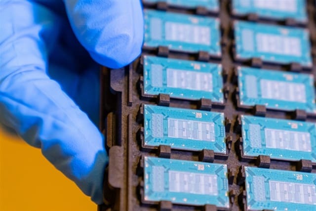
Intel Corporation has entered a strategic collaboration with Lens Technology, a China-based manufacturer, to advance semiconductor packaging using glass substrates. The partnership marks a significant cross-border effort to develop materials that could replace traditional organic substrates in high-performance chip designs.
The two companies will explore manufacturing techniques and process development for glass-based packaging solutions. This technology aims to address growing demands for higher interconnect density and improved power delivery in computing platforms, according to Intel.
Why Glass Matters for Chip Performance
Glass substrates offer several advantages over conventional organic materials used in chip packaging today. The material enables finer wiring patterns and tighter spacing between connections, which becomes critical as chipmakers push transistor counts higher and seek to stack components more densely.
Thermal stability is another key benefit. Glass can withstand higher processing temperatures and exhibits lower warpage during manufacturing, reducing defects and improving yield rates. For power-hungry AI accelerators and data center processors, better thermal management translates directly to performance gains.
Intel has been vocal about its glass substrate roadmap, positioning the technology as essential for chips beyond the current decade. The company expects glass packaging to support future architectures that demand thousands of input/output connections per square millimeter.
Lens Technology's Manufacturing Footprint
Lens Technology brings substantial manufacturing scale to the partnership. The company operates production facilities across mainland China and has experience in precision glass processing, primarily for consumer electronics. Its capacity in glass fabrication and chemical strengthening processes could accelerate Intel's pathway to volume production.
The collaboration also carries geopolitical nuance. Semiconductor supply chains have become increasingly regionalized, with Western chipmakers balancing technology leadership against manufacturing partnerships in Asia. Intel's choice to work with a Chinese manufacturer reflects the continued interdependence of global chip ecosystems, even as export controls tighten on advanced lithography and design tools.
For Lens Technology, the partnership represents a strategic pivot toward higher-margin semiconductor materials. The company has faced revenue pressures in its core smartphone cover glass business as device upgrade cycles slow. Semiconductor packaging offers a growth avenue with longer-term contracts and less exposure to consumer demand volatility.
Roadmap and Competitive Context
Intel has not disclosed a timeline for commercial deployment of glass substrates, but industry observers expect pilot production lines within three to four years. The company is likely targeting its Xeon server processors and future AI accelerators as initial applications, where performance gains justify the higher material costs.
Competitors are also exploring advanced packaging. TSMC continues to refine its chip-on-wafer-on-substrate approach, while Samsung has invested in panel-level fan-out technologies. Glass substrates remain a longer-term bet, requiring new equipment sets and process integration that few manufacturers have mastered.
The Intel-Lens collaboration will focus on process feasibility and cost modeling. Key technical challenges include drilling microvias through glass without cracking, depositing thin metal layers uniformly, and integrating glass panels with existing assembly lines. Success in these areas could reshape the economics of high-performance chip packaging and shift where future fabs are built.
What Comes Next
Both companies plan to establish joint development teams and share intellectual property related to glass substrate manufacturing. Intel will contribute packaging architecture expertise and process specifications, while Lens Technology will provide materials engineering and production scale-up capabilities.
The partnership underscores a broader industry shift toward heterogeneous integration, where multiple chiplets and memory dies are combined in a single package. Glass substrates could enable denser configurations and lower latency between components, critical for workloads that move massive datasets between processors and memory.
As the collaboration progresses, Intel's ability to bring glass packaging to market will depend on yield improvements and cost reductions. The technology must compete not only on performance but also on total cost of ownership for server and AI system builders. If successful, the partnership could establish new supply chain anchors in Asia and redefine the materials stack for chips powering the next decade of computing.
RELATED STORIES

China's Chip Makers Split Three Ways Beneath the Revenue Growth
Tran Quoc Bao · 3 min
JCET Eyes $968 Million to Scale AI Packaging Lines
Tran Quoc Bao · 3 min
Kioxia Pushes Flash Memory to Replace DRAM Amid Market Squeeze
Jun-ho Seo · 3 min
Sharpa Secures $668 Million at $3.3 Billion Valuation in Tech Giant-Backed Round
Cheng Wei-Lun · 2 min
Spot something wrong? Email editor@briefasia.com. We log every correction publicly.