Technology · Dev
Intel Unveils EMIB-T Packaging to Challenge TSMC's CoWoS Dominance
As transistor scaling hits physical limits, chipmakers turn to advanced packaging innovation to sustain AI accelerator performance gains
KEY TAKEAWAYS
- ·Intel introduced EMIB-T packaging technology to compete with TSMC's CoWoS platform as transistor density scaling slows across the industry.
- ·Multiple chipmakers presented new packaging approaches at IEEE ECTC, signaling that packages themselves are hitting physical and thermal limits.
- ·Advanced packaging capacity remains concentrated in Asia, with TSMC in Taiwan, Intel in Malaysia, and Samsung scaling capabilities in South Korea.
The New Battleground
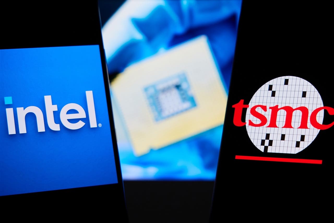
Intel has introduced EMIB-T, a packaging technology designed to compete directly with TSMC's established CoWoS platform, as the semiconductor industry confronts the slowing pace of transistor density improvements. The move signals a strategic pivot across chipmakers, who are increasingly betting on packaging innovation rather than pure transistor scaling to deliver performance gains in AI accelerators and high-performance computing.
The announcement came during presentations at this year's IEEE Electronic Components and Technology Conference, where Intel, Marvell, and TSMC each outlined distinct packaging roadmaps. According to SemiAnalysis, the conference revealed that advanced packages themselves are now approaching physical and thermal limits, forcing engineers to rethink interconnect density, power delivery, and thermal management at the package level.
What EMIB-T Brings
Intel's EMIB-T builds on its existing Embedded Multi-die Interconnect Bridge technology, which uses small silicon bridges to connect chiplets at high bandwidth without requiring a full interposer. The "T" variant is understood to target tighter pitch interconnects and higher die-to-die bandwidth, specifications critical for the memory-intensive workloads that dominate AI training and inference.
TSMC's CoWoS, or Chip-on-Wafer-on-Substrate, has been the packaging architecture of choice for Nvidia's recent GPU generations and other leading AI chips. CoWoS uses a silicon interposer to connect logic dies with high-bandwidth memory stacks, enabling the data throughput required for large language models and neural network training. Intel's EMIB approach has historically offered cost advantages by using localized bridges rather than a full interposer, but has lagged in bandwidth density for the most demanding applications.
Industry-Wide Shift
The conference presentations underscore a broader industry consensus that Moore's Law, in its traditional form, no longer drives the performance curve. Transistor nodes below 3nm deliver diminishing returns in density and power efficiency, while costs escalate sharply. Packaging has emerged as the primary lever for performance, allowing chipmakers to combine specialized dies, integrate memory closer to compute, and manage power and thermals more effectively than monolithic designs permit.
Marvell's presentations at the conference focused on custom interconnect solutions for data center and networking applications, reflecting the company's emphasis on tailored silicon for hyperscale customers. TSMC, meanwhile, detailed enhancements to its CoWoS family and explored next-generation substrate materials to address thermal bottlenecks as power densities climb above 1,000 watts per package in some AI accelerator designs.
Asia's Central Role
The packaging competition is centered squarely in Asia. TSMC's advanced packaging capacity is concentrated in Taiwan, with expansion plans in progress to meet surging demand from AI chip designers. Intel operates packaging facilities in Malaysia and has committed investment to expand its advanced packaging footprint in the region, viewing it as essential to competing for hyperscale and AI customers.
Samsung, though not detailed in the conference roundup, is also scaling its own advanced packaging capabilities in South Korea, adding another dimension to regional competition. The geographic concentration of cutting-edge packaging capacity in Northeast and Southeast Asia raises supply chain considerations for Western chip designers and governments pursuing semiconductor self-sufficiency.
What Comes Next
Intel's EMIB-T remains in the development phase, with commercial availability and customer adoption timelines not yet disclosed. The technology's success will depend on whether it can match or exceed CoWoS in bandwidth density and thermal performance while delivering on Intel's traditional cost advantage. For AI chip designers, packaging choice is now as consequential as process node selection, with implications for performance, cost, and time to market.
The conference discussions also highlighted emerging constraints. As packages grow larger and integrate more dies, substrate warpage, thermal dissipation, and power delivery integrity become limiting factors. Chipmakers are exploring new materials, including glass substrates and advanced thermal interface materials, to push these boundaries further. The next wave of packaging innovation will likely involve not just interconnect density, but holistic system-level co-design of silicon, package, and cooling.
RELATED STORIES
Taiwan Indicts Nvidia Manager in Chip-Smuggling Investigation
Cheng Wei-Lun · 4 min
Integrated Systems Will Drive Next Wave of AI Growth, Says TSMC
Cheng Wei-Lun · 4 min

Manila's Chip Industry Still Stalled in Assembly While Taipei Built Fabs
Priyanka V. Rao · 4 min

Xiaomi Unveils 3nm Mobile Processor to Challenge Qualcomm and MediaTek
Cheng Wei-Lun · 3 min
Spot something wrong? Email editor@briefasia.com. We log every correction publicly.