Technology · Dev
Huawei Bets on System Architecture Over Transistor Density in AI Chip Race
Chinese tech giant's 18-tier design philosophy challenges conventional semiconductor scaling as US export controls reshape Asia's chip competition
KEY TAKEAWAYS
- ·Huawei introduced an 18-tier design framework emphasizing system architecture, data throughput and hardware-software coordination over traditional transistor density.
- ·The strategy reflects constraints from US export controls that limit Huawei's access to advanced manufacturing nodes and packaging techniques.
- ·The approach addresses the memory wall bottleneck in AI workloads, where data movement between chips often limits performance more than processor speed.
A Different Path to Performance
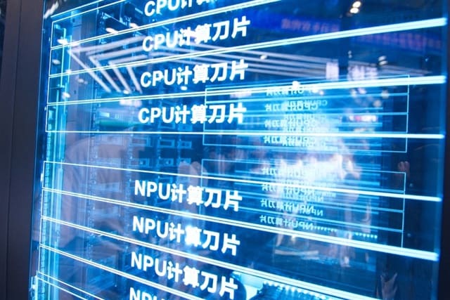
Huawei has unveiled a design philosophy it calls the "18-tier pagoda," a reference to the multi-layered approach the company is taking to semiconductor performance at a time when traditional transistor scaling delivers diminishing returns. The strategy places system architecture, data throughput and coordination between hardware and software at the center of AI chip development, according to the company.
The approach represents a departure from the roadmap that has dominated the industry for decades. Where competitors have focused on packing more transistors into smaller spaces, Huawei is arguing that the next leap in computational power will come from how chips communicate with each other and with the software layers above them.
The shift comes as Huawei remains cut off from leading-edge manufacturing nodes and advanced packaging techniques due to US export restrictions. The company has been forced to design around these constraints, and the 18-tier framework reflects that reality. Rather than compete on process node alone, Huawei is betting that smarter system integration can close the performance gap.
Rethinking the Stack
The 18-tier model breaks the traditional hardware-software divide into granular layers, each optimized for a specific function in the AI workload pipeline. Huawei is focusing on faster data movement between compute units, tighter integration between chips and AI models, and software that can dynamically allocate resources based on workload characteristics.
This is not purely a hardware play. The company is building co-design frameworks that allow AI researchers to influence chip behavior at a lower level than typical application programming interfaces permit. The goal is to reduce latency and improve utilization rates, metrics that matter as much as raw compute power in large-scale AI deployments.
Huawei has not disclosed specific performance benchmarks or named the chips that embody this philosophy, but the announcement signals a strategic repositioning. The company is framing its limitations as an opportunity to rethink assumptions that have guided chip design since the beginning of the Moore's Law era.
Asia's Diverging Chip Strategies
The move fits into a broader pattern across Asian semiconductor players. As access to cutting-edge tools and nodes becomes politicized, companies in China are investing in alternative architectures, domain-specific accelerators and software optimization. Huawei's emphasis on system-level performance echoes efforts by other Chinese AI labs and chipmakers to extract more from older process nodes.
Meanwhile, competitors in South Korea, Taiwan and Japan continue to push conventional scaling through advanced packaging and next-generation lithography. TSMC is expanding capacity for 3-nanometer and preparing for 2-nanometer production, while Samsung is accelerating its foundry roadmap to capture AI chip orders. These firms are betting that access to leading-edge manufacturing remains the primary competitive advantage.
The divergence creates two parallel tracks in Asia's semiconductor landscape. One prioritizes access to the most advanced fabrication technology. The other seeks performance through architectural innovation and tighter vertical integration. Both paths are responses to the same pressure: the insatiable demand for AI compute and the geopolitical fractures that now shape who can build what.
The Data Movement Bottleneck
Huawei's focus on data movement addresses a real constraint in modern AI systems. Training and inference workloads are increasingly limited by how quickly data can move between memory and compute units, not by the speed of the processors themselves. This bottleneck, known as the memory wall, has driven the industry toward high-bandwidth memory and chiplet designs that place memory closer to logic.
Huawei's 18-tier approach extends this thinking across the entire system. The company is designing for scenarios where hundreds or thousands of chips work in concert, and where the efficiency of inter-chip communication can determine overall throughput. In large language model training, for example, gradient synchronization across distributed nodes often consumes more time than the forward and backward passes through the model.
If Huawei can demonstrate meaningful performance gains from system-level optimization, it may shift the conversation in Asia's AI chip market. Customers care about total cost of ownership and time-to-result, not just transistor counts. A chip that delivers competitive performance on older nodes with better power efficiency and lower latency could find traction, especially in markets where access to the latest Nvidia or AMD accelerators is restricted or expensive.
Implications for the Regional Ecosystem
Huawei's strategy has ripple effects across the supply chain. Emphasis on advanced packaging, interposers and high-speed interconnects benefits companies in Taiwan, South Korea and Japan that supply these components. The shift toward co-design between hardware and AI frameworks also creates demand for software engineering talent and partnerships with research institutions across Asia.
At the same time, the 18-tier model underscores the fragmentation of the AI chip market. Standardization, which has historically driven economies of scale in semiconductors, becomes harder when different players optimize for different constraints. Huawei's chips may excel in environments where its software stack is deeply integrated, but struggle in ecosystems built around other platforms.
The broader question is whether architectural innovation can substitute for process leadership in the long run. History suggests that manufacturing advantage compounds over time. But the current moment, with AI workloads evolving rapidly and geopolitical barriers reshaping access, may offer a window for alternative approaches to gain ground.
Huawei's pagoda is a gamble that the industry's center of gravity is shifting from the fab to the system. Whether that bet pays off will depend on execution, market adoption and the durability of the export controls that shaped the strategy in the first place.
RELATED STORIES
Huawei Unveils Sub-800-Gram Laptop Running Homegrown Kirin Chip
Cheng Wei-Lun · 3 min

Asia's Memory Makers Shift Focus as DRAM Margins Challenge HBM Dominance
Cheng Wei-Lun · 4 min
SK Hynix Eyes Stake Sale in $3 Billion China Packaging Facility
Cheng Wei-Lun · 2 min

GlobalFoundries Posts Stronger Second-Quarter Results on AI Optics Demand
Cheng Wei-Lun · 4 min
Spot something wrong? Email editor@briefasia.com. We log every correction publicly.